TMS320DM6437
Digital Media Processor
www.ti.com
SPRS345B–NOVEMBER 2006–REVISED MARCH 2007
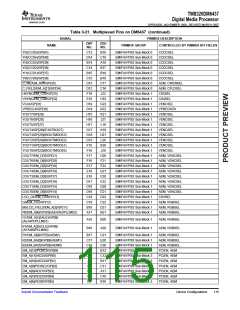
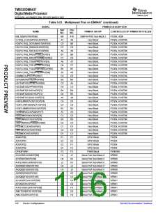
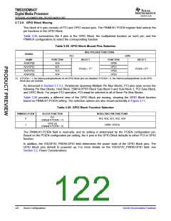
3.7.3.2 Peripherals Spanning Multiple Pin Mux Blocks
Some peripherals span multiple Pin Mux Blocks. To use these peripherals, they must be selected in all of
the relevant Pin Mux Blocks. The following is the list of peripherals that span multiple Pin Mux Blocks:
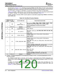
•
PCI: PCI pins span across the Host Block, EMIFA/VPSS Block Sub-Block 0 and Sub-Block 3, PCI
Data Block, and GPIO Block. To select PCI pins, program PINMUX registers as follows:
–
–
Host Block: PCIEN = 1, HOSTBK = 000
EMIFA/VPSS Block: Select either Major Configuration Option F or G. For more details on the
PINMUX settings associated with Major Configuration Options F or G, see Section 3.7.3.13,
EMIFA/VPSS BLock Muxing.
–
–
PCI Data Block: PCIEN = 1
GPIO Block: PCIEN = 1
•
•
McBSP0: Six McBSP0 pins are located in the Serial Port Sub-Block 0, but the CLKS0 pin is muxed in
the Timer0 Block. To select McBSP0 pins, program PINMUX registers as follows:
–
–
Serial Port Sub-Block 0: SPBK0 = 01
Timer0 Block: If CLKS0 pin is desired, program TIM0BK = 10 or 11.
McBSP1: Six McBSP1 pins are located in the Serial Port Sub-Block 1, but the CLKS1 pin is muxed in
the Timer0 Block. To select McBSP1 pins, program PINMUX registers as follows:
–
Serial Port Sub-Block 1: SPBK1 = 01 (if both McBSP1 transmit and receive pins are needed) or
11 (if only McBSP1 transmit pins are needed)
–
Timer0 Block: If CLKS1 pin is desired, program TIM0BK = 10.
•
UART0: The two UART0 data pins are located in the UART0 Data Block, but the two UART0 flow
control pins are located in the UART0 Flow Control Block. To select UART0, program PINMUX
registers as follows:
–
–
UART0 Data Block: UR0BK = 1
UART0 Flow Control Block: If flow control pins are desired, program UR0FCBK = 01.
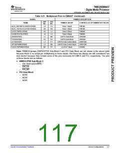
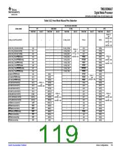
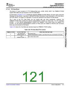
3.7.3.3 Host Block Muxing
This block of 27 pins consists of PCI, HPI, VLYNQ, EMAC, MDIO, and GPIO muxed pins. The following
register fields select the pin functions in the Host Block:
•
•
PINMUX1.PCIEN
PINMUX1.HOSTBK
Table 3-22 summarizes the 27 pins in the Host Block, the multiplexed function on each pin, and the
PINMUX configurations to select the corresponding function.
118
Device Configurations
Submit Documentation Feedback

 TI [ TEXAS INSTRUMENTS ]