TMS320DM6437
Digital Media Processor
www.ti.com
SPRS345B–NOVEMBER 2006–REVISED MARCH 2007
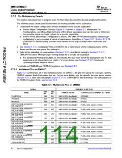
3.7.3 Pin Multiplexing Details
This section discusses how to program each Pin Mux Block to select the desired peripheral functions.
The following steps can be used to determine pin muxing suitable for the application:
1. Understand the major configuration choices available for the specific application.
a. Device Major Configuration Choices: Figure 3-11 shown in Section 3.7, Multiplexed Pin
Configurations, provides a high-level view of the device pin muxing and can be used to determine
the possible mix of peripheral options for a specific application.
b. EMIFA/VPSS Block Major Configuration Choices: The EMIFA/VPSS block features extensive pin
multiplexing to accommodate a variety of applications. In addition to Figure 3-11, Section 3.7.3.13,
EMIFA/VPSS Block Muxing, provides more details on the Major Configuration choices for this
block.
2. See Section 3.7.3.1, Multiplexed Pins on DM6437, for a summary of all the multiplexed pins on this
device and the pin mux group they belong to.
3. Refer to the individual pin mux sections (Section 3.7.3.3, Host Block Muxing to Section 3.7.3.13,
EMIFA/VPSS Block Muxing) for pin muxing details for a specific pin mux block.
a. For peripherals that span multiple pin mux blocks, the user must select the appropriate pins for that
peripheral in all relevant pin mux blocks. For more details, see Section 3.7.3.2, Peripherals
Spanning Multiple Pin Mux Blocks.
For details on PINMUX0 and PINMUX1 registers, see Section 3.7.2.
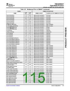
3.7.3.1 Multiplexed Pins on DM6437
Table 3-21 summarizes all of the multiplexed pins on DM6437, the pin mux group for each pin, and the
PINMUX register fields that control the pin. For pin mux details, see the specific pin mux group section
(Section 3.7.3.3, Host Block Muxing to Section 3.7.3.13, EMIFA/VPSS Block Muxing). For a description of
the PINMUX register fields, see Section 3.7.2.
Table 3-21. Multiplexed Pins on DM6437
SIGNAL
PINMUX DESCRIPTION
CONTROLLED BY PINMUX BIT FIELDS
ZWT
NO.
ZDU
NO.
NAME
PINMUX GROUP
PCLK/GP[54]
VD/GP[53]
HD/GP[52]
A14
A13
A15
A18
A17
A19
EMIFA/VPSS Sub-Block 0
EMIFA/VPSS Sub-Block 0
EMIFA/VPSS Sub-Block 0
CCDCSEL
HVDSEL
HVDSEL
CI7(CCD15)/EM_A[13]/AD25/
EM_D[0]/GP[51]
B10
A10
B11
C11
A11
D11
B12
C12
A12
A13
C13
B13
B14
A14
C14
C15
EMIFA/VPSS Sub-Block 0
EMIFA/VPSS Sub-Block 0
EMIFA/VPSS Sub-Block 0
EMIFA/VPSS Sub-Block 0
EMIFA/VPSS Sub-Block 0
EMIFA/VPSS Sub-Block 0
EMIFA/VPSS Sub-Block 0
EMIFA/VPSS Sub-Block 0
PCIEN, AEM, AEAW, CI76SEL
PCIEN, AEM, AEAW, CI76SEL
PCIEN, AEM, AEAW, CI54SEL
PCIEN, AEM, AEAW, CI54SEL
PCIEN, AEM, AEAW, CI32SEL
PCIEN, AEM, AEAW, CI32SEL
PCIEN, AEM, AEAW, CI10SEL
PCIEN, AEM, AEAW, CI10SEL
CI6(CCD14)/EM_A[14]/AD27/
EM_D[1]/GP[50]
CI5(CCD13)/EM_A[15]/AD29/
EM_D[2]/GP[49]
CI4(CCD12)/EM_A[16]/PGNT/
EM_D[3]/GP[48]
CI3(CCD11)/EM_A[17]/AD31/
EM_D[4]/GP[47]
CI2(CCD10)/EM_A[18]/PRST/
EM_D[5]/GP[46]
CI1(CCD9)/EM_A[19]/PREQ/
EM_D[6]/GP[45]
CI0(CCD8)/EM_A[20]/PINTA/
EM_D[7]/GP[44]
YI7(CCD7)/GP[43]
YI6(CCD6)/GP[42]
A12
B13
A15
B15
EMIFA/VPSS Sub-Block 0
EMIFA/VPSS Sub-Block 0
CCDCSEL
CCDCSEL
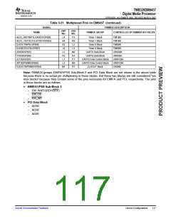
114
Device Configurations
Submit Documentation Feedback

 TI [ TEXAS INSTRUMENTS ]