TMS320DM6437
Digital Media Processor
www.ti.com
SPRS345B–NOVEMBER 2006–REVISED MARCH 2007
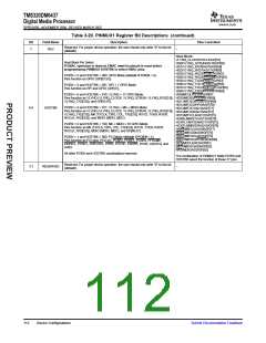
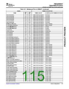
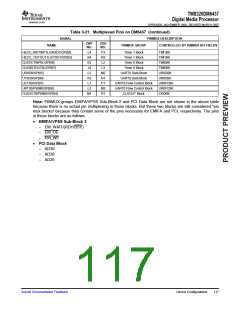
Table 3-20. PINMUX1 Register Bit Descriptions (continued)
Bit
Field Name
Description
Pins Controlled
Host Block:
See list of 27 pins in HOSTBK bit field
description
PCI Data Block:
AD26
AD28
AD30
GPIO Block:
AD0/GP[0]
AD1/GP[1]
AD2/GP[2]
AD4/GP[3]
PCI Enable.
The PINMUX1.PCIEN reflects the state of the PCIEN pin. PINMUX1.PCIEN is
read only and cannot be modified by software. For proper device
operation, the user must hold the desired setting at the PCIEN pin
throughout device operation.
EMIFA/VPSS Sub-Block 0*:
CI7(CCD15)/EM_A[13]/AD25/EM_D[0]/GP[51]
CI6(CCD14)/EM_A[14]/AD27/EM_D[1]/GP[50]
CI5(CCD13)/EM_A[15]/AD29/EM_D[2]/GP[49]
CI4(CCD12)/EM_A[16]/PGNT/EM_D[3]/GP[48]
CI3(CCD11)/EM_A[17]/AD31/EM_D[4]/GP[47]
PCIEN = 0: No PCI supported. Internal pullup/pulldown (IPU/IPD) on these pins
are enabled.
For PCI multiplexed pins in the GPIO Block, when PCIEN = 0, the pins function CI2(CCD10)/EM_A[18]/PRST/EM_D[5]/GP[46]
as GPIO (GP[3:0]). CI1(CCD9)/EM_A[19]/PREQ/EM_D[6]/GP[45]
For PCI multiplexed pins in the Host Block, refer to PINMUX1.HOSTBK field for CI0(CCD8)/EM_A[20]/PINTA/EM_D[7]/GP[44]
the actual pin functions.
0
PCIEN
EMIFA/VPSS Sub-Block 3*:
For PCI multiplexed pins in the EMIFA/VPSS Block, refer to PINMUX0.AEM,
AEAW, CI76SEL, CI54SEL, CI32SEL, and CI10SEL fields for the actual pin
functions.
For PCI pins in the PCI Data Block, when PCIEN = 0, the pins have no function
and should be left unconnected.
EM_A[12]/PCBE3/GP[89]
EM_A[11]/AD24/GP[90]
EM_A[10]/AD23/GP[91]
EM_A[9]/PIDSEL/GP[92]
EM_A[8]/AD21/GP[93]
PCIEN = 1: PCI supported. Internal pullup/pulldown (IPU/IPD) on all PCI pins
are disabled.
EM_A[7]/AD22/GP[94]
EM_A[6]/AD20/GP[95]
EM_A[5]/AD19/GP[96]
All pins function as PCI pins.
Applicable only for PINMUX0.AEM = 000b or 101b.
The pin mux for the EMIFA/VPSS Sub-Block 0
and EMIFA/VPSS Sub-Block 3 pins are
controlled by a combination of PCIEN and other
PINMUX0/1 fields, including HOSTBK, AEM,
AEAW, CI76SEL, CI54SEL, CI32SEL, and
CI10SEL. See Section 3.7.3.13.7, EMIFA/VPSS
Block Pin-By-Pin Multiplexing Summary, for the
full set of valid configurations of EMIFA/VPSS
Block pins.
For the full set of valid configurations of Host
Block pins, see Section 3.7.3.3, Host Block
Muxing.
Submit Documentation Feedback
Device Configurations
113

 TI [ TEXAS INSTRUMENTS ]