TMS320C6678
Multicore Fixed and Floating-Point Digital Signal Processor
SPRS691D—April 2013
www.ti.com
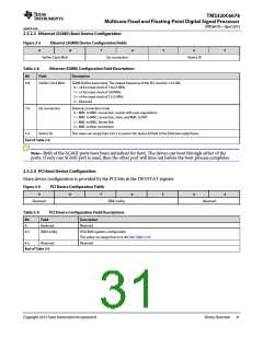
Table 2-16
EMIF16 Boot Mode Parameter Table
Byte
Offset
Configured Through Boot
Configuration Pins
Name
Description
20
Chip Select
Chip Select for the NOR flash
Memory width of the Emif16 bus (16 bits)
-
22
Memory Width
Wait Enable
-
24
Extended wait mode enabled
0 = Wait enable is disabled
1 = Wait enable is enabled
YES
End of Table 2-16
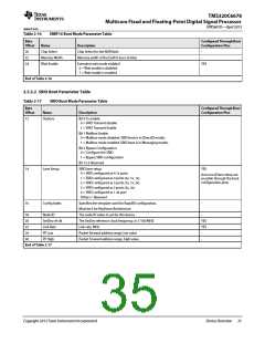
2.5.3.2 SRIO Boot Parameter Table
Table 2-17
SRIO Boot Mode Parameter Table
Byte
Offset
Configured Through Boot
Configuration Pins
Name
Description
12
Options
Bit 0 Tx enable
-
0 = SRIO Transmit disable
1 = SRIO Transmit Enable
Bit 1 Mailbox Enable
0 = Mailbox mode disabled. SRIO boot is in DirectIO mode).
1 = Mailbox mode enabled. SRIO boot is in Messaging mode).
Bit 2 Bypass Configuration
0 = Configure the SRIO
1 = Bypass SRIO configuration
Bit 15-3 Reserved
14
16
Lane Setup
SRIO lane setup
YES
0 = SRIO configured as 4 1x ports
1 = SRIO configured as 3 ports (2x, 1x, 1x)
2 = SRIO configured as 3 ports (1x, 1x, 2x)
3 = SRIO configured as 2 ports (2x, 2x)
4 = SRIO configured as 1 4x port
Others = Reserved
(but not all lane setup are
possible through the boot
configuration pins)
Config Index
Specifies the template used for RapidIO configuration.
Must be 0 for KeyStone Architecture
The node ID value to set for this device
The SerDes reference clock frequency, in 1/100 MHZ
Link rate, MHz
-
18
20
22
24
26
Node ID
-
SerDes ref clk
Link Rate
PF Low
YES
YES
Packet forward address range, low value
Packet Forward address range, high value
-
-
PF High
End of Table 2-17
Copyright 2013 Texas Instruments Incorporated
Device Overview 35

 TI [ TEXAS INSTRUMENTS ]