TMS320C6678
Multicore Fixed and Floating-Point Digital Signal Processor
SPRS691D—April 2013
www.ti.com
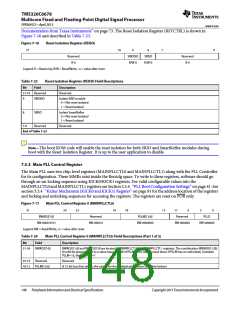
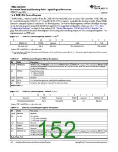
Documentation from Texas Instruments’’ on page 73. The Reset Isolation Register (RSTCTRL) is shown in
Figure 7-16 and described in Table 7-23.
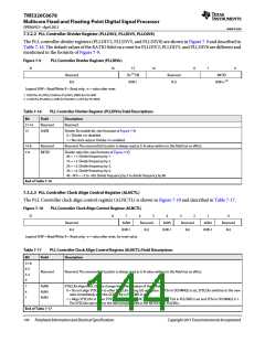
Figure 7-16
Reset Isolation Register (RSISO)
31
10
9
8
7
0
Reserved
R-0
SRIOISO
R/W-0
SRISO
R/W-0
Reserved
R-0
Legend: R = Read only; R/W = Read/Write; -n = value after reset
Table 7-23
Reset Isolation Register (RSISO) Field Descriptions
Bit
Field
Description
31-10 Reserved
Reserved.
9
SRIOISO
Isolate SRIO module
0 = Not reset isolated
1 = Reset Isolated
8
SRISO
Isolate SmartReflex
0 = Not reset isolated
1 = Reset Isolated
7-0
Reserved
Reserved.
End of Table 7-23
Note—The boot ROM code will enable the reset isolation for both SRIO and SmartReflex modules during
boot with the Reset Isolation Register. It is up to the user application to disable.
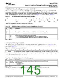
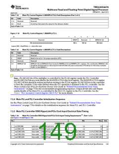
7.5.3 Main PLL Control Register
The Main PLL uses two chip-level registers (MAINPLLCTL0 and MAINPLLCTL1) along with the PLL Controller
for its configuration. These MMRs exist inside the Bootcfg space. To write to these registers, software should go
through an un-locking sequence using KICK0/KICK1 registers. For valid configurable values into the
MAINPLLCTL0 and MAINPLLCTL1 registers see Section 2.5.4 ‘‘PLL Boot Configuration Settings’’ on page 41. See
section 3.3.4 ‘‘Kicker Mechanism (KICK0 and KICK1) Register’’ on page 81 for the address location of the registers
and locking and unlocking sequences for accessing the registers. The registers are reset on POR only.
Figure 7-17
Main PLL Control Register 0 (MAINPLLCTL0)
31
24
23
19
18
12
11
Reserved
RW-000000
6
5
0
BWADJ[7:0]
RW-0000 0101
Legend: RW = Read/Write; -n = value after reset
Reserved
PLLM[12:6]
PLLD
RW-000000
RW-0000 0
RW-0000000
Table 7-24
Main PLL Control Register 0 (MAINPLLCTL0) Field Descriptions (Part 1 of 2)
Bit
Field Description
31-24
BWADJ[7:0]
BWADJ[11:8] and BWADJ[7:0] are located in MAINPLLCTL0 and MAINPLLCTL1 registers. The combination (BWADJ[11:0])
should be programmed to a value equal to half of PLLM[12:0] value (round down if PLLM has an odd value). Example:
PLLM=15, then BWADJ=7
23-19
18-12
Reserved
Reserved
PLLM[12:6]
A 13-bit bus that selects the values for the multiplication factor (see Note below)
148
Peripheral Information and Electrical Specifications
Copyright 2013 Texas Instruments Incorporated

 TI [ TEXAS INSTRUMENTS ]