TMS320C6678
Multicore Fixed and Floating-Point Digital Signal Processor
SPRS691D—April 2013
www.ti.com
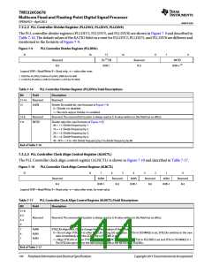
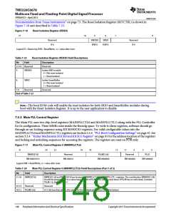
7.5.2.2 PLL Controller Divider Register (PLLDIV2, PLLDIV5, PLLDIV8)
The PLL controller divider registers (PLLDIV2, PLLDIV5, and PLLDIV8) are shown in Figure 7-9 and described in
Table 7-16. The default values of the RATIO field on a reset for PLLDIV2, PLLDIV5, and PLLDIV8 are different and
mentioned in the footnote of Figure 7-9.
Figure 7-9
PLL Controller Divider Register (PLLDIVn)
31
16
15
14
8
7
0
Reserved
R-0
Dn (1) EN
Reserved
R-0
RATIO
R/W-1
R/W-n (2)
Legend: R/W = Read/Write; R = Read only; -n = value after reset
1 D2EN for PLLDIV2; D5EN for PLLDIV5; D8EN for PLLDIV8
2 n=02h for PLLDIV2; n=04h for PLLDIV5; n=3Fh for PLLDIV8
Table 7-16
PLL Controller Divider Register (PLLDIVn) Field Descriptions
Description
Bit
Field
Reserved
31-16
15
Reserved.
DnEN
Divider Dn enable bit. (see footnote of Figure 7-9)
0 = Divider n is disabled.
1 = No clock output. Divider n is enabled.
14-8
7-0
Reserved
RATIO
Reserved. The reserved bit location is always read as 0. A value written to this field has no effect.
Divider ratio bits. (see footnote of Figure 7-9)
0h = ÷1. Divide frequency by 1.
1h = ÷2. Divide frequency by 2.
2h = ÷3. Divide frequency by 3.
3h = ÷4. Divide frequency by 4.
4h - 4Fh = ÷5 to ÷80. Divide frequency by 5 to divide frequency by 80.
End of Table 7-16
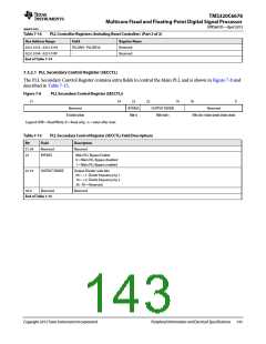
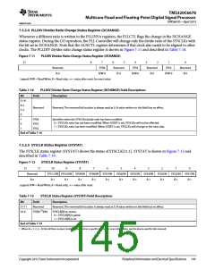
7.5.2.3 PLL Controller Clock Align Control Register (ALNCTL)
The PLL Controller clock align control register (ALNCTL) is shown in Figure 7-10 and described in Table 7-17.
Figure 7-10
PLL Controller Clock Align Control Register (ALNCTL)
31
8
7
6
5
4
3
2
1
0
Reserved
R-0
ALN8
R/W-1
Reserved
R-0
ALN5
R/W-1
Reserved
R-0
ALN2
R/W-1
Reserved
R-0
Legend: R/W = Read/Write; R = Read only; -n = value after reset, for reset value
Table 7-17
PLL Controller Clock Align Control Register (ALNCTL) Field Descriptions
Bit
31-8
6-5
3-2
0
Field Description
Reserved
Reserved. The reserved bit location is always read as 0. A value written to this field has no effect.
7
ALN8
ALN5
ALN2
SYSCLKn alignment. Do not change the default values of these fields.
0 = Do not align SYSCLKn to other SYSCLKs during GO operation. If SYSn in DCHANGE is set, SYSCLKn switches to the new
ratio immediately after the GOSET bit in PLLCMD is set.
1 = Align SYSCLKn to other SYSCLKs selected in ALNCTL when the GOSET bit in PLLCMD is set and SYSn in DCHANGE is 1.
The SYSCLKn rate is set to the ratio programmed in the RATIO bit in PLLDIVn.
4
1
End of Table 7-17
144
Peripheral Information and Electrical Specifications
Copyright 2013 Texas Instruments Incorporated

 TI [ TEXAS INSTRUMENTS ]