TMS320C6672
Multicore Fixed and Floating-Point Digital Signal Processor
SPRS708C—February 2012
www.ti.com
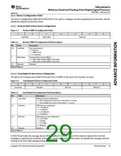
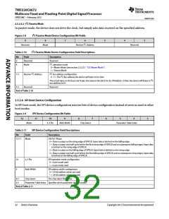
2.5.2.5.2 I2C Passive Mode
In passive mode, the device does not drive the clock, but simply acks data received on the specified address.
Figure 2-8
9
I2C Passive Mode Device Configuration Bit Fields
8
7
6
5
4
3
Reserved
Mode
Receive I2C Address
Reserved
Table 2-10
I2C Passive Mode Device Configuration Field Descriptions
Description
Bit
9
Field
Reserved
Reserved
8
Mode
I2C operation mode
0 = Master Mode (See section 2.5.2.5.1 ‘‘I2C Master Mode’’)
1 = Passive Mode
7-5
4-3
Receive I2C Address
I2C bus address configuration
0 - 7 = The I2C Bus address the device will listen to for data
The actual value on the bus is 0x19 plus the value in bits [8:5]. For Ex. if bits[8:5] = 0 then the device will listen to I2C
bus address 0x19.
Reserved
Reserved
End of Table 2-10
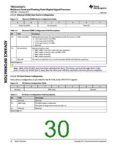
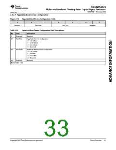
2.5.2.6 SPI Boot Device Configuration
In SPI boot mode, the SPI device configuration uses ten bits of device configuration instead of seven as used in other
boot modes.
Figure 2-9
12
SPI Device Configuration Bit Fields
11
10
9
8
7
6
5
4
3
Mode
4, 5 Pin
Addr Width
Chip Select
Parameter Table Index
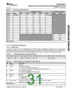
Table 2-11
SPI Device Configuration Field Descriptions
Bit
Field
Description
12-11
Mode
Clk Pol / Phase
0 = Data is output on the rising edge of SPICLK. Input data is latched on the falling edge.
1 = Data is output one half-cycle before the first rising edge of SPICLK and on subsequent falling edges. Input data
is latched on the rising edge of SPICLK.
2 = Data is output on the falling edge of SPICLK. Input data is latched on the rising edge.
3 = Data is output one half-cycle before the first falling edge of SPICLK and on subsequent rising edges. Input data
is latched on the falling edge of SPICLK.
10
9
4, 5 Pin
SPI operation mode configuration
0 = 4-pin mode used
1 = 5-pin mode used
Addr Width
Chip Select
SPI address width configuration
0 = 16-bit address values are used
1 = 24-bit address values are used
8-7
6-3
The chip select field value
Parameter Table Index Specifies which parameter table is loaded
End of Table 2-11
32
Device Overview
Copyright 2012 Texas Instruments Incorporated

 TI [ TEXAS INSTRUMENTS ]