TMS320C6672
Multicore Fixed and Floating-Point Digital Signal Processor
SPRS708C—February 2012
www.ti.com
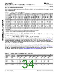
2.5.3 PLL Boot Configuration Settings
The PLL default settings are determined by the BOOTMODE[12:10] bits. The table below shows settings for various
input clock frequencies.
Table 2-13
C66x DSP System PLL Configuration (1)
800 MHz Device 1000 MHz Device 1200 MHz Device 1250 MHz Device 1500 MHz Device PASS PLL = 350 MHz (2)
0b000 50.00
0b001 66.67
0b010 80.00
0b011 100.00
0
0
0
0
31
23
19
15
800
0
0
0
0
4
0
4
39
29
24
19
63
7
1000
1000.05
1000
1000
1000
1000
1000
0
0
0
0
47
35
29
23
1200
0
0
0
0
31
23
19
15
800
0
0
1
0
4
0
4
4
59 1500
44 1500.075
74 1500
29 1500
95 1500
11 1500
47 1500
0
1
3
0
41
1050
800.04
800
1200.06
1200
800.04
800
62
1050.053
1050
104
20
800
1200
800
1050
0b100 156.25 24 255 800
0b101 250.00 31 800
24 383 1200
47 1200
24 191 1200
24 255 800
31 800
24 335
41
24 167
1050
4
4
4
4
1050
0b110 312.50 24 127 800
0b111 122.88 47 624 800
End of Table 2-13
31
24 127 800
47 624 800
1050
28 471 999.989 31 624 1200
121 1499.14 11 204
1049.6
1 The PLL boot configuration of initial silicon 1.0 may only support 800MHz, 1000MHz and 1200MHz frequencies by default.
2 The PASS PLL generates 1050 MHz and is internally divided by 3 to feed 350 MHz to the packet accelerator.
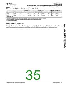
OUTPUT_DIVIDE is the value of the field of SECCTL[22:19]. This will set the PLL to the maximum clock setting
for the device (with OUTPUT_DIVIDE=2, by default).
CLK = CLKIN × (PLLM+1) ÷ (OUTPUT_DIVIDE × (PLLD+1))
The configuration for the PASS PLL is also shown. The PASS PLL is configured with these values only if the Ethernet
boot mode is selected with the input clock set to match the main PLL clock (not the PASS clock). See Table 2-3 for
details on configuring Ethernet boot mode. The output from the PASS PLL goes through an on-chip divider to
reduce the operating frequency before reaching the NETCP. The PASS PLL generates 1050 MHz, and after the chip
divider (=3), feeds 350 MHz to the NETCP.
The Main PLL is controlled using a PLL controller and a chip-level MMR. The DDR3 PLL and PASS PLL are
controlled by chip level MMRs. For details on how to set up the PLL see section 7.5 ‘‘Main PLL and PLL Controller’’
on page 132. For details on the operation of the PLL controller module, see the Phase Locked Loop (PLL) Controller
for KeyStone Devices User Guide in ‘‘Related Documentation from Texas Instruments’’ on page 69.
Table 2-14
C66x DSP System PLL Configuration Part 2 (1) (Part 1 of 2)
1250 MHz Device
PLLM DSP ƒ
49
1500 MHz Device
PLLM DSP ƒ
59 1500
PASS PLL = 350 MHz (2)
PLLD PLLM
DSP ƒ (3)
0 41 1050
BOOTMODE
[12:10]
Input Clock
Freq (MHz)
PLLD
PLLD
0b000
0b001
0b010
0b011
0b100
0b101
50.00
0
1250
1250.06
1250
1250
0
66.67
1
3
0
0
0
74
124
24
15
9
0
1
0
4
0
44
74
29
95
11
1500.075
1500
1
62
1050.053
1050
80.00
3
104
20
100.00
156.25
250.00
1500
0
1050
1250
1500
24
4
335
41
1050
1250
1500
1050
34
Device Overview
Copyright 2012 Texas Instruments Incorporated

 TI [ TEXAS INSTRUMENTS ]