TMS320C6672
Multicore Fixed and Floating-Point Digital Signal Processor
SPRS708C—February 2012
www.ti.com
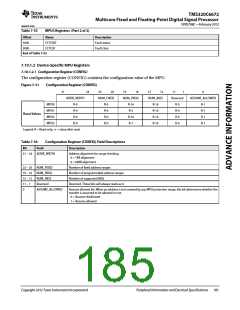
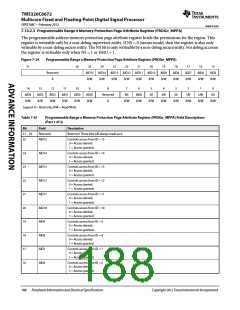
7.10.2.3 Programmable Range n Memory Protection Page Attribute Register (PROGn_MPPA)
The programmable address memory protection page attribute register holds the permissions for the region. This
register is writeable only by a non-debug supervisor entity. If NS = 0 (secure mode) then the register is also only
writeable by a non-debug secure entity. The NS bit is only writeable by a non-debug secure entity. For debug accesses
the register is writeable only when NS = 1 or EMU = 1.
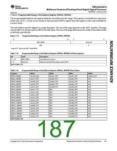
Figure 7-34
Programmable Range n Memory Protection Page Attribute Register (PROGn_MPPA)
31
26
25
24
23
22
21
20
19
18
17
16
15
Reserved
R
AID15 AID14 AID13 AID12 AID11 AID10
AID9
R/W
AID8
R/W
AID7
R/W
AID6
R/W
AID5
R/W
R/W
R/W
R/W
R/W
R/W
R/W
14
13
12
11
10
9
8
7
6
5
4
3
2
1
0
AID4
R/W
AID3
R/W
AID2
R/W
AID1
R/W
AID0
R/W
AIDX
R/W
Reserved
R
NS
EMU
R/W
SR
SW
R/W
SX
UR
UW
R/W
UX
R/W
R/W
R/W
R/W
R/W
Legend: R = Read only; R/W = Read/Write
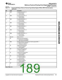
Table 7-61
Programmable Range n Memory Protection Page Attribute Register (PROGn_MPPA) Field Descriptions
(Part 1 of 2)
Bit
Field
Description
31 – 26
25
Reserved
AID15
Reserved. These bits will always reads as 0.
Controls access from ID = 15
0 = Access denied.
1 = Access granted.
24
23
22
21
20
19
18
17
16
AID14
AID13
AID12
AID11
AID10
AID9
Controls access from ID = 14
0 = Access denied.
1 = Access granted.
Controls access from ID = 13
0 = Access denied.
1 = Access granted.
Controls access from ID = 12
0 = Access denied.
1 = Access granted.
Controls access from ID = 11
0 = Access denied.
1 = Access granted.
Controls access from ID = 10
0 = Access denied.
1 = Access granted.
Controls access from ID = 9
0 = Access denied.
1 = Access granted.
AID8
Controls access from ID = 8
0 = Access denied.
1 = Access granted.
AID7
Controls access from ID = 7
0 = Access denied.
1 = Access granted.
AID6
Controls access from ID = 6
0 = Access denied.
1 = Access granted.
188
Peripheral Information and Electrical Specifications
Copyright 2012 Texas Instruments Incorporated

 TI [ TEXAS INSTRUMENTS ]