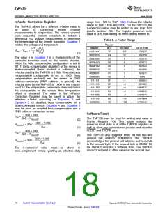
TMP435
SBOS495A –MARCH 2010–REVISED APRIL 2010
www.ti.com
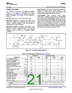
1
9
1
9
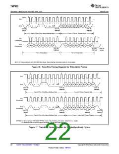
SCL
¼
SDA
1
0
0
1
1
0
0(1) R/W
P7 P6 P5 P4 P3
P2 P1
P0
¼
Start By
Master
ACK By
ACK By
TMP435
TMP435
Frame 2 Pointer Register Byte
Frame 1 Two- Wire Slave Address Byte
1
9
1
9
SCL
(Continued)
SDA
D7 D6 D5 D4 D3 D2 D1 D0
D7 D6 D5 D4 D3 D2 D1 D0
(Continued)
ACK By
ACK By
Stop By
Master
TMP435
TMP435
Frame 3 Data Byte 1
Frame 4 Data Byte 2
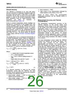
NOTE (1): Slave address 1001100 (TMP435) shown. See Ordering Information table for more details.
Figure 16. Two-Wire Timing Diagram for Write Word Format
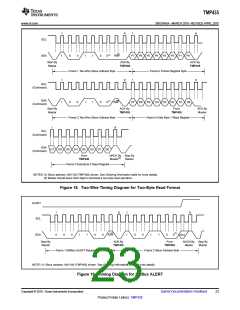
1
9
1
9
SCL
SDA
1
0
0
1
1
0
0(1)
R/W
P7
P6
P5
P4
P3
P2
P1
P0
Start By
Master
ACK By
ACK By
TMP435
TMP435
Frame 1 Two-Wire Slave Address Byte
Frame 2 Pointer Register Byte
1
9
1
9
SCL
(Continued)
SDA
1
0
0(1)
1
0
0
1
R/W
D7
D6
D5
D4 D3
D2
D1
D0
(Continued)
Start By
Master
ACK By
From
TMP435
NACK By
Master(2)
TMP435
Frame 3 Two-Wire Slave Address Byte
Frame 4 Data Byte 1 Read Register
NOTES: (1) Slave address 1001100 (TMP435) shown. See Ordering Information table for more details.
(2) Master should leave SDA high to terminate a single-byte read operation.
Figure 17. Two-Wire Timing Diagram for Single-Byte Read Format
22
Submit Documentation Feedback
Copyright © 2010, Texas Instruments Incorporated
Product Folder Link(s): TMP435

 TI [ TEXAS INSTRUMENTS ]