TMP112
www.ti.com ......................................................................................................................................................... SBOS473B–MARCH 2009–REVISED JUNE 2009
NOISE
Start Data Transfer: A change in the state of the
SDA line, from high to low, while the SCL line is high,
defines a START condition. Each data transfer is
initiated with a START condition.
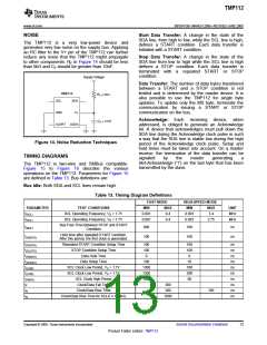
The TMP112 is
a very low-power device and
generates very low noise on the supply bus. Applying
an RC filter to the V+ pin of the TMP112 can further
reduce any noise that the TMP112 might propagate
to other components. RF in Figure 14 should be less
than 5kΩ and CF should be greater than 10nF.
Stop Data Transfer: A change in the state of the
SDA line from low to high while the SCL line is high
defines a STOP condition. Each data transfer is
terminated with
condition.
a
repeated START or STOP
Supply Voltage
Data Transfer: The number of data bytes transferred
between a START and a STOP condition is not
limited and is determined by the master device. It is
also possible to use the TMP112 for single byte
updates. To update only the MS byte, terminate the
TMP112
R
F £ 5kW
SCL
SDA
V+
communication by issuing
communication on the bus.
a START or STOP
GND
Acknowledge: Each receiving device, when
addressed, is obliged to generate an Acknowledge
bit. A device that acknowledges must pull down the
SDA line during the Acknowledge clock pulse in such
a way that the SDA line is stable low during the high
period of the Acknowledge clock pulse. Setup and
hold times must be taken into account. On a master
receive, the termination of the data transfer can be
CF ³ 10nF
ALERT ADD0
Figure 14. Noise Reduction Techniques
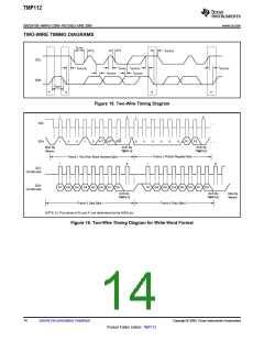
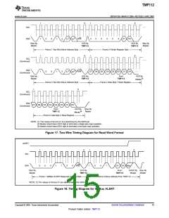
TIMING DIAGRAMS
signaled
by
the
master
generating
a
Not-Acknowledge ('1') on the last byte that has been
transmitted by the slave.
The TMP112 is two-wire and SMBus compatible.
Figure 15 to Figure 18 describe the various
operations on the TMP112. Parameters for Figure 15
are defined in Table 13. Bus definitions are:
Bus Idle: Both SDA and SCL lines remain high.
Table 13. Timing Diagram Definitions
FAST MODE
HIGH-SPEED MODE
PARAMETER
f(SCL)
TEST CONDITIONS
MIN
MAX
0.4
MIN
MAX
3.4
UNIT
MHz
MHz
SCL Operating Frequency, VS > 1.7V
SCL Operating Frequency, VS < 1.7V
0.001
0.001
0.001
0.001
f(SCL)
0.4
2.75
Bus Free Time Between STOP and START
Condition
t(BUF)
600
100
160
100
ns
ns
Hold time after repeated START condition.
After this period, the first clock is generated.
t(HDSTA)
t(SUSTA)
t(SUSTO)
t(HDDAT)
t(SUDAT)
t(LOW)
t(LOW)
t(HIGH)
tF
Repeated START Condition Setup Time
STOP Condition Setup Time
Data Hold Time
100
100
0
100
100
0
ns
ns
ns
ns
ns
ns
ns
ns
ns
ns
Data Setup Time
100
1300
1300
600
10
SCL Clock Low Period, VS > 1.7V
SCL Clock Low Period, VS < 1.7V
SCL Clock High Period
160
200
60
Clock/Data Fall Time
300
300
tR
Clock/Data Rise Time
160
tR
Clock/Data Rise Time for SCLK ≤ 100kHz
1000
Copyright © 2009, Texas Instruments Incorporated
Submit Documentation Feedback
13
Product Folder Link(s): TMP112

 TI [ TEXAS INSTRUMENTS ]