TMP112
www.ti.com ......................................................................................................................................................... SBOS473B–MARCH 2009–REVISED JUNE 2009
1
9
1
9
¼
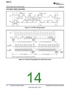
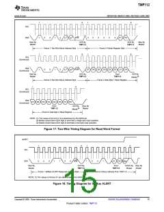
SCL
SDA
1
0
0
1
0
A1(1) A0(1)
R/W
0
0
0
0
0
0
P1
P0
Start By
Master
ACK By
ACK By
Stop By
Master
TMP112
TMP112
Frame 1 Two-Wire Slave Address Byte
Frame 2 Pointer Register Byte
1
9
1
9
SCL
¼
(Continued)
SDA
A1(1) A0(1)
¼
0
1
0
0
1
R/W
D7
D6
D5
D4 D3
D2
D1
D0
(Continued)
Start By
Master
ACK By
From
TMP112
ACK By
Master(2)
TMP112
Frame 3 Two-Wire Slave Address Byte
Frame 4 Data Byte 1 Read Register
1
9
SCL
(Continued)
SDA
D7 D6
D5
D4
D3
D2
D1
D0
(Continued)
From
ACK By
Master(3)
Stop By
Master
TMP112
Frame 5 Data Byte 2 Read Register
NOTE: (1) The values of A0 and A1 are determined by the ADD0 pin.
(2) Master should leave SDA high to terminate a single-byte read operation.
(3) Master should leave SDA high to terminate a two-byte read operation.
Figure 17. Two-Wire Timing Diagram for Read Word Format
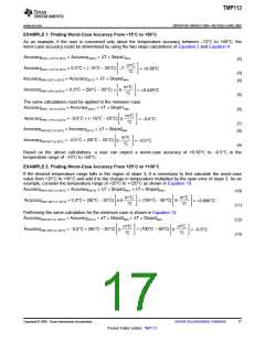
ALERT
SCL
1
9
1
9
SDA
0
0
0
1
1
0
0
R/W
1
0
0
1
A1
A0 Status
Start By
Master
ACK By
From
TMP112
NACK By Stop By
Master Master
TMP112
Frame 1 SMBus ALERT Response Address Byte
Frame 2 Slave Address From TMP112
NOTE: (1) The values of A0 and A1 are determined by the ADD0 pin.
Figure 18. Timing Diagram for SMBus ALERT
Copyright © 2009, Texas Instruments Incorporated
Submit Documentation Feedback
15
Product Folder Link(s): TMP112

 TI [ TEXAS INSTRUMENTS ]