TMP112
www.ti.com ......................................................................................................................................................... SBOS473B–MARCH 2009–REVISED JUNE 2009
Both operating modes are represented in Figure 13.
Table 10 and Table 11 describe the format for the
THIGH and TLOW registers. Note that the most
significant byte is sent first, followed by the least
significant byte. Power-up reset values for THIGH and
TLOW are:
SERIAL INTERFACE
The TMP112 operates as a slave device only on the
two-wire bus and SMBus. Connections to the bus are
made via the open-drain I/O lines SDA and SCL. The
SDA and SCL pins feature integrated spike
suppression filters and Schmitt triggers to minimize
the effects of input spikes and bus noise. The
TMP112 supports the transmission protocol for both
fast (1kHz to 400kHz) and high-speed (1kHz to
3.4MHz) modes. All data bytes are transmitted MSB
first.
•
•
THIGH = +80°C
TLOW = +75°C
The format of the data for THIGH and TLOW is the same
as for the Temperature Register.
Table 10. Bytes 1 and 2 of THIGH Register(1)
SERIAL BUS ADDRESS
BYTE
D7
D6
D5
D4
H8
D3
H7
D2
H6
D1
H5
D0
H4
To communicate with the TMP112, the master must
first address slave devices via a slave address byte.
The slave address byte consists of seven address
bits, and a direction bit indicating the intent of
executing a read or write operation.
H11
H10
H9
1
(H12) (H11) (H10)
(H9)
(H8)
(H7)
(H6)
(H5)
BYTE
D7
H3
D6
H2
D5
H1
D4
H0
D3
0
D2
0
D1
0
D0
0
2
(H4)
(H3)
(H2)
(H1)
(H0)
(0)
(0)
(0)
The TMP112 features an address pin to allow up to
four devices to be addressed on a single bus.
Table 12 describes the pin logic levels used to
properly connect up to four devices.
(1) Extended mode 13-bit configuration shown in parenthesis.
Table 11. Bytes 1 and 2 of TLOW Register(1)
BYTE
D7
D6
D5
D4
L8
D3
L7
D2
L6
D1
L5
D0
L4
Table 12. Address Pin and Slave Addresses
L11
L10
L9
1
DEVICE TWO-WIRE
(L12) (L11) (L10)
(L9)
(L8)
(L7)
(L6)
(L5)
ADDRESS
1001000
1001001
1001010
1001011
A0 PIN CONNECTION
BYTE
D7
L3
D6
L2
D5
L1
D4
L0
D3
0
D2
0
D1
0
D0
0
Ground
V+
2
(L4)
(L3)
(L2)
(L1)
(L0)
(0)
(0)
(0)
SDA
SCL
(1) Extended mode 13-bit configuration shown in parenthesis.
BUS OVERVIEW
WRITING/READING OPERATION
The device that initiates the transfer is called a
master, and the devices controlled by the master are
slaves. The bus must be controlled by a master
device that generates the serial clock (SCL), controls
the bus access, and generates the START and STOP
conditions.
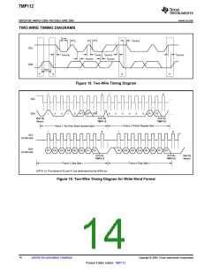
Accessing a particular register on the TMP112 is
accomplished by writing the appropriate value to the
Pointer Register. The value for the Pointer Register is
the first byte transferred after the slave address byte
with the R/W bit low. Every write operation to the
TMP112 requires a value for the Pointer Register
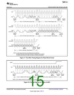
(see Figure 16).
To address a specific device, a START condition is
initiated, indicated by pulling the data-line (SDA) from
a high to low logic level while SCL is high. All slaves
on the bus shift in the slave address byte on the
rising edge of the clock, with the last bit indicating
whether a read or write operation is intended. During
the ninth clock pulse, the slave being addressed
responds to the master by generating an
Acknowledge and pulling SDA low.
When reading from the TMP112, the last value stored
in the Pointer Register by a write operation is used to
determine which register is read by a read operation.
To change the register pointer for a read operation, a
new value must be written to the Pointer Register.
This action is accomplished by issuing a slave
address byte with the R/W bit low, followed by the
Pointer Register byte. No additional data are
required. The master can then generate a START
condition and send the slave address byte with the
R/W bit high to initiate the read command. See
Figure 17 for details of this sequence. If repeated
Data transfer is then initiated and sent over eight
clock pulses followed by an Acknowledge Bit. During
data transfer SDA must remain stable while SCL is
high, because any change in SDA while SCL is high
is interpreted as a START or STOP signal.
Once all data have been transferred, the master
generates a STOP condition indicated by pulling SDA
from low to high, while SCL is high.
Copyright © 2009, Texas Instruments Incorporated
Submit Documentation Feedback
11
Product Folder Link(s): TMP112

 TI [ TEXAS INSTRUMENTS ]