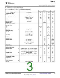
TMP112
www.ti.com ......................................................................................................................................................... SBOS473B–MARCH 2009–REVISED JUNE 2009
POINTER REGISTER
TEMPERATURE REGISTER
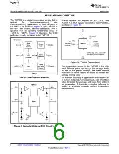
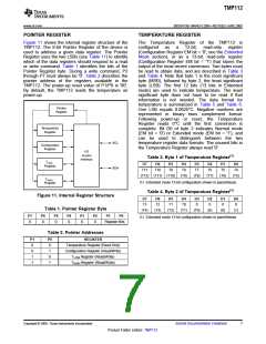
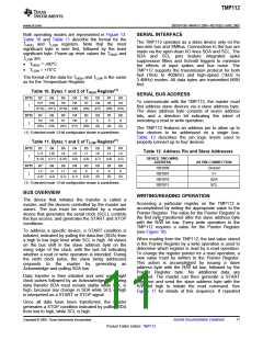
Figure 11 shows the internal register structure of the
TMP112. The 8-bit Pointer Register of the device is
used to address a given data register. The Pointer
Register uses the two LSBs (see Table 11) to identify
which of the data registers should respond to a read
or write command. Table 1 identifies the bits of the
Pointer Register byte. During a write command, P2
through P7 must always be '0'. Table 2 describes the
pointer address of the registers available in the
TMP112. The power-up reset value of P1/P0 is '00'.
By default, the TMP112 reads the temperature on
power-up.
The Temperature Register of the TMP112 is
configured as
a
12-bit, read-only register
(Configuration Register EM bit = '0'; see the Extended
Mode section), or as a 13-bit, read-only register
(Configuration Register EM bit = '1') that stores the
output of the most recent conversion. Two bytes must
be read to obtain data, and are described in Table 3
and Table 4. Note that byte 1 is the most significant
byte (MSB), followed by byte 2, the least significant
byte (LSB). The first 12 bits (13 bits in Extended
mode) are used to indicate temperature. The least
significant byte does not have to be read if that
information is not needed. The data format for
temperature is summarized in Table 5 and Table 6.
One LSB equals 0.0625°C. Negative numbers are
represented in binary twos complement format.
Following power-up or reset, the Temperature
Register reads 0°C until the first conversion is
complete. Bit D0 of byte 2 indicates Normal mode
(EM bit = '0') or Extended mode (EM bit = '1'), and
can be used to distinguish between the two
temperature register data formats. The unused bits in
the Temperature Register always read '0'.
Pointer
Register
Temperature
Register
SCL
Configuration
Register
I/O
Control
Table 3. Byte 1 of Temperature Register(1)
Interface
TLOW
Register
D7
D6
D5
D4
T8
D3
T7
D2
T6
D1
T5
D0
T4
SDA
T11
T10
T9
(T12) (T11) (T10)
(T9)
(T8)
(T7)
(T6)
(T5)
THIGH
(1) Extended mode 13-bit configuration shown in parentheses.
Register
Table 4. Byte 2 of Temperature Register(1)
Figure 11. Internal Register Structure
Table 1. Pointer Register Byte
D7
T3
D6
T2
D5
T1
D4
T0
D3
0
D2
0
D1
0
D0
0
(T4)
(T3)
(T2)
(T1)
(T0)
(0)
(0)
(1)
P7
P6
P5
P4
P3
P2
P1
P0
(1) Extended mode 13-bit configuration shown in parentheses.
0
0
0
0
0
0
Register Bits
Table 2. Pointer Addresses
P1
P0
0
REGISTER
0
0
1
1
Temperature Register (Read Only)
Configuration Register (Read/Write)
TLOW Register (Read/Write)
1
0
1
THIGH Register (Read/Write)
Copyright © 2009, Texas Instruments Incorporated
Submit Documentation Feedback
7
Product Folder Link(s): TMP112

 TI [ TEXAS INSTRUMENTS ]