TMDS361
SLLS919–DECEMBER 2008............................................................................................................................................................................................ www.ti.com
TMDS DDC and Local I2C Pins
DDC I2C Buffer or Repeater: The TMDS361 provides buffering on the DDC I2C interface for each of the input
ports connected. This feature isolates the capacitance on the source side from the sink side and thus helps in
passing system-level compliance. See the DDC I2C Function Description section for a detailed description on
how the DDC I2C buffer operates. Note that a key requirement on the sink side is that the VIL(Sink) (input to
TMDS361) should be less than 0.4 V. This requirement should be met for the DDC I2C buffer to function
properly. There are three settings of VIL(Sink) and VOL(Sink) that can be chosen based on OVS settings (See Table 8
through Table 11).
Local I2C Interface: The TMDS361 includes a slave I2C interface to control device features like TMDS input port
selection, TMDS output edge-rate control, power management, DDC buffer OVS settings, etc. See Table 8
through Table 11.
The TMDS361 is designed to be controlled via a local I2C interface or GPIO interface, based on the status of the
I2C_SEL pin. The local I2C interface in the TMDS361 is only a slave I2C interface. See the I2C INTERFACE
NOTES section for a detailed description of I2C functionality.
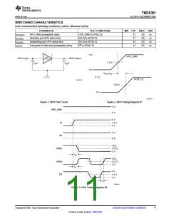
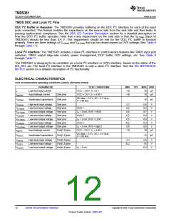
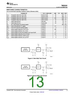
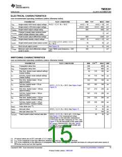
ELECTRICAL CHARACTERISTICS
over recommended operating conditions (unless otherwise noted)
PARAMETER
Low-level input current
Input leakage current
TEST CONDITIONS
VCC = 3.6 V, VI = 0 V
MIN
–10
–10
TYP
MAX UNIT
IL
10
10
µA
µA
Ilkg(Sink)
Sink pins
Sink pins
VCC = 3.6 V, VI = 4.95 V
DC bias = 2.5 V, AC = 3.5 Vp-p,
f = 100 kHz
CIO(Sink)
Input/output capacitance
15
pF
VIH(Sink)
VIL1(Sink)
VOL1(Sink)
VIL2(Sink)
VOL2(Sink)
VIL3(Sink)
VOL3(Sink)
Ilkg(I2C)
High-level input voltage
Low-level input voltage
Low-level output voltage
Low-level input voltage
Low-level output voltage
Low-level input voltage
Low-level output voltage
Input leakage current
Sink pins
Sink pins
Sink pins
Sink pins
Sink pins
Sink pins
Sink pins
Port[1:3] pins
2.1
–0.2
0.6
5.5
0.4
0.7
0.4
0.6
0.3
0.5
10
V
V
OVS 1
IO = 3 mA, OVS = HIGH
OVS 2
V
–0.2
0.5
V
IO = 3 mA, OVS = LOW
OVS 3
V
–0.2
0.4
V
IO = 3 mA, OVS = high-Z
VCC = 3.6 V, VI = 4.95 V
V
–10
µA
DC bias = 2.5 V, AC = 3.5 Vp-p,
f = 100 kHz
CIO(I2C)
Input/output capacitance
Port[1:3] pins
15
pF
VIH(I2C)
VIL(I2C)
VOL(I2C)
High-level input voltage
Low-level input voltage
Low-level output voltage
Port[1:3] pins
Port[1:3] pins
Port[1:3] pins
2.1
5.5
1.5
0.2
V
V
V
–0.2
IO = 3 mA
12
Submit Documentation Feedback
Copyright © 2008, Texas Instruments Incorporated
Product Folder Link(s) :TMDS361

 TI [ TEXAS INSTRUMENTS ]