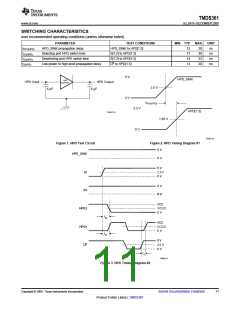
TMDS361
www.ti.com ............................................................................................................................................................................................ SLLS919–DECEMBER 2008
ELECTRICAL CHARACTERISTICS
over recommended operating conditions (unless otherwise noted)
PARAMETER
TEST CONDITIONS
MIN TYP
AVCC – 10
MAX UNIT
VOH
VOL
Single-ended HIGH-level output voltage AVCC = 3.3 V, RT = 50 Ω
AVCC + 10
mV
mV
mV
Single-ended LOW-level output voltage
AVCC – 600
400
AVCC – 400
600
VSWING Single-ended output voltage swing
Change in steady-state common-mode
VOC(SS)
5
mV
output voltage between logic states
VOD(pp) Peak-to-peak output differential voltage
V(O)SBY Single-ended standby output voltage
800
1200
mV
mV
AVCC – 10
AVCC + 10
0 V ≤ VCC ≤ 1.5 V, AVCC = 3.3 V,
RT = 50 Ω
I(O)OFF
Single-ended power-down output current
–10
10
15
µA
IOS
Short-circuit output current
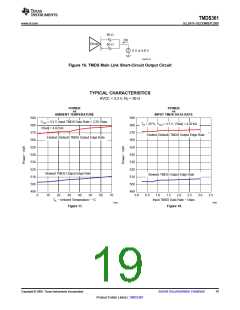
See Figure 16
-15
12
mA
mV
VCD(pp) Minimum valid clock differential voltage
(peak-to-peak)
Input TMDS clock frequency = 300
MHz
100
SWITCHING CHARACTERISTICS
over recommended operating conditions (unless otherwise noted)
PARAMETER
Propagation delay time
Propagation delay time
TEST CONDITIONS
MIN TYP(1)
MAX UNIT
tPLH
tPHL
tR1
250
250
800
800
140
ps
ps
ps
Rise time, fastest mode (default setting):
Fastest Setting
84
110
110
160
160
210
210
230
230
tF1
tR2
tF2
tR3
tF3
tR4
tF4
Fall time, fastest mode (default setting):
Fastest Setting
84
140
190
190
230
230
260
260
ps
ps
ps
ps
ps
ps
ps
Rise time, fastest mode + 50 ps
(approximately)
142
142
187
187
216
216
Fall time, fastest mode + 50 ps
(approximately)
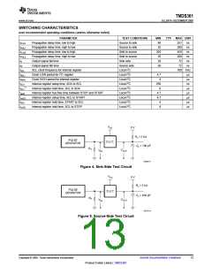
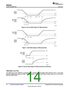
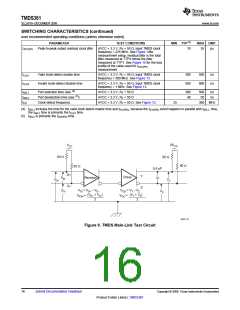
AVCC = 3.3 V, RT = 50 Ω. See Figure 9 and
Figure 10.
Rise time, fastest mode + 100 ps
(approximately)
Fall time, fastest mode + 100 ps
(approximately)
Rise time, fastest mode + 120 ps
(approximately): Slowest Setting
Fall time, fastest mode + 120 ps
(approximately): Slowest Setting
(2)
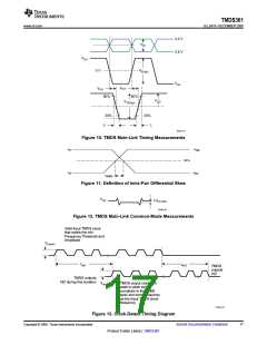
tSK(P)
Pulse skew (see
Intra-pair skew
)
8
15
30
ps
ps
ps
ps
tSK(D)
AVCC = 3.3 V, RT = 50 Ω. See Figure 11.
10
(3)
tSK(O)
tJITD(PP)
Inter-pair skew (see
)
100
88
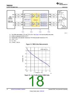
Peak-to-peak output residual data jitter
AVCC = 3.3 V, RT = 50 Ω, dR = 2.25 Gbps.
See Figure 14 for measurement setup;
residual jitter is the total jitter measured at
TTP4 minus the jitter measured at TTP1. See
Figure 15 for the loss profile of the cable used
for tJITD(PP) measurement. Also see Typical
Curves for tJITD(PP) across cable length and
input TMDS data rate.
40
(1) All typical values are at 25°C and with a 3.3-V supply.
(2) tsk(p) is the magnitude of the time difference between tPLH and tPHL of a specified terminal.
(3) tsk(o) is the magnitude of the difference in propagation delay times between any specified terminals of a sink-port bank when inputs of
the active source port are tied together.
Copyright © 2008, Texas Instruments Incorporated
Submit Documentation Feedback
15
Product Folder Link(s) :TMDS361

 TI [ TEXAS INSTRUMENTS ]