TMDS361
SLLS919–DECEMBER 2008............................................................................................................................................................................................ www.ti.com
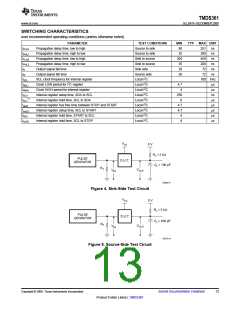
SWITCHING CHARACTERISTICS (continued)
over recommended operating conditions (unless otherwise noted)
PARAMETER
TEST CONDITIONS
MIN TYP(1)
MAX UNIT
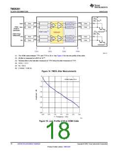
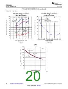
tJITC(PP)
Peak-to-peak output residual clock jitter
AVCC = 3.3 V, RT = 50 Ω, input TMDS clock
frequency = 225 MHz. See Figure 14for
measurement setup; residual jitter is the total
jitter measured at TTP4 minus the jitter
measured at TTP1. See Figure 15 for the loss
profile of the cable used for tJITC(PP)
measurement.
10
35
ps
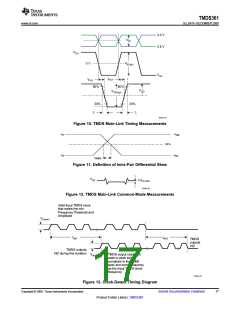
tCLK1
tCLK2
Valid clock-detect enable time
Invalid clock-detect disable time
AVCC = 3.3 V, RT = 50 Ω, input TMDS clock
frequency = 300 MHz. See Figure 13.
300
500
500
800
ns
ns
AVCC = 3.3 V, RT = 50 Ω, input TMDS clock
frequency = 1 MHz. See Figure 13.
(4)
tSEL1
tSEL2
fCD
Port selection time (see
AVCC = 3.3 V, RT = 50 Ω
300
500
50
ns
ns
(5)
Port deselection time (see
Clock-detect frequency
)
AVCC = 3.3 V, RT = 50 Ω
40
AVCC = 3.3 V, RT = 50 Ω. See Figure 13.
25
300
MHz
(4) tSEL1 includes the time for the valid clock detect enable time and tS1(HPD), because the tS1(HPD) event happens in parallel with tSEL1; thus,
the tSEL1 time is primarily the tCLK1 time.
(5) tSEL2 is primarily the tS2(HPD) time.
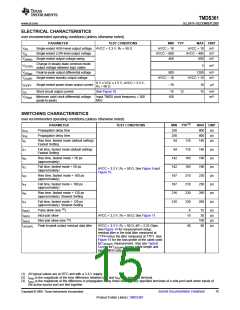
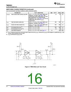
AVCC
VCC
50 W
50 W
50 W
50 W
0.5 pF
D+
D–
Y
Z
Driver
Receiver
VID
VD+
VY
VID = VD+ – VD–
VOD = VY – VZ
VD–
VZ
(VD+ + VD–
)
(VY + VZ)
2
VICM
=
VOC =
2
S0371-01
Figure 9. TMDS Main-Link Test Circuit
16
Submit Documentation Feedback
Copyright © 2008, Texas Instruments Incorporated
Product Folder Link(s) :TMDS361

 TI [ TEXAS INSTRUMENTS ]