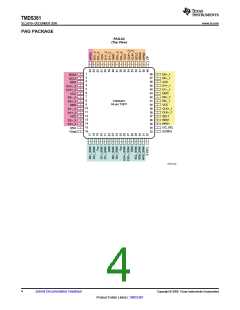
TMDS361
SLLS919–DECEMBER 2008............................................................................................................................................................................................ www.ti.com
Table 2. Control-Pin Lookup Table(1)
SIGNAL
LEVEL
STATE
DESCRIPTION
Normal operational mode for device. If LP is left floating, then a weak internal pullup to VCC
pulls it to VCC.
H
Normal mode
LP
Low-power
mode
Device is forced into a low-power state, causing the inputs and outputs to go to a
high-impedance state. All other inputs are ignored.
L
S2
S1
H
L
H
H
L
Port 1
Port 2
Port 3
Port 1 is selected as the active port; all other ports are low.
Port 2 is selected as the active port; all other ports are low.
Port 3 is selected as the active port; all other ports are low.
S[2:1]
GPIO
mode
L
HPD[1:3] follow
HPD_SINK
L
H
Standby mode: HPD[1:3] follow HPD_sink.
Device is configured by I2C logic.
L
I2C
I2C_SEL
VSadj
Device is configured by GPIO. If the I2C_SEL pin is left floating, then a weak internal pullup to
VCC pulls the I2C_SEL pin high.
H
GPIO
Driver output voltage swing precision control to aid with system compliance. The VSadj
resistor value can be selected to be 4.02 kΩ ±10% based on the system requirement to pass
HDMI compliance.
Compliant
voltage
4.02 kΩ
(1) (H) Logic high; (L) Logic low
ORDERING INFORMATION(1)
PART NUMBER
TMDS361PAGR
TMDS361PAGT
PART MARKING
TMDS361
PACKAGE
64-pin TQFP reel (large)
64-pin TQFP reel (small)
TMDS361
(1) For the most current package and ordering information, see the Package Option Addendum at the end of this document, or see the TI
Web site at www.ti.com.
ABSOLUTE MAXIMUM RATINGS
over operating free-air temperature range (unless otherwise noted)(1)
VALUE
–0.3 to 3.6
–0.3 to 4
–0.3 to 5.5
–0.3 to 5.5
±10,000
UNIT
Supply voltage range(2)
Voltage range
VCC
V
TMDS I/O
HPD and DDC I/O
Control and status I/O
Human body model(3) on SCL[1:3], SDA[1:3], HPD[1:3], D[0:2]+_[1:3],
D[0:2]–_[1:3], CLK+_[1:3], CLK–_[1:3] pins
V
Electrostatic discharge
Human body model(3) on all other pins
Charged-device model(4)
Machine model(5)
±9,000
±1500
±200
V
IEC 61000-4-2(6), contact discharge
IEC 61000-4-2(6), air discharge
±8,000
±15,000
Continuous power dissipation
See Dissipation Ratings table
(1) Stresses beyond those listed under Absolute Maximum Ratings may cause permanent damage to the device. These are stress ratings
only, and functional operation of the device at these or any other conditions beyond those indicated under Recommended Operating
Conditions is not implied. Exposure to absolute-maximum-rated conditions for extended periods may affect device reliability.
(2) All voltage values, except differential voltages, are with respect to network ground terminal.
(3) Tested in accordance with JEDEC Standard 22, Test Method A114-B
(4) Tested in accordance with JEDEC Standard 22, Test Method C101-A
(5) Tested in accordance with JEDEC Standard 22, Test Method A115-A
(6) Tested in accordance with IEC EN 61000-4-2
8
Submit Documentation Feedback
Copyright © 2008, Texas Instruments Incorporated
Product Folder Link(s) :TMDS361

 TI [ TEXAS INSTRUMENTS ]