TLK10002
SLLSE75 –MAY 2011
www.ti.com
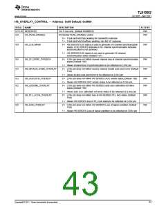
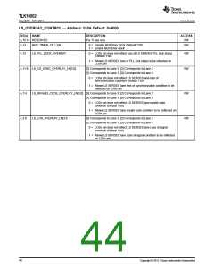
LS_OVERLAY_CONTROL — Address: 0x0A Default: 0x4000
BIT(s)
NAME
DESCRIPTION
ACCESS
RW
A.15:14 RESERVED
For TI use only
A.13
A.12
BER_TIMER_CLK_EN
LS_PLL_LOCK_OVERLAY
0 = Disable BER timer clock (Default 1’b0)
1 = Enable BER timer clock
RW
0 = LOSx pin does not reflect loss of LS SERDES PLL lock status
RW
RW
(Default 1’b0)
1 = Allows LS SERDES loss of PLL lock status to be reflected on
LOSx pin
A.11:8 LS_CH_SYNC_OVERLAY_LN[3:0]
[3] Corresponds to Lane 3, [2] Corresponds to Lane 2
[1] Corresponds to Lane 1, [0] Corresponds to Lane 0
0 = LOSx pin does not reflect LS SERDES lane loss of
synchronization condition (Default 1’b0)
1 = Allows LS SERDES lane loss of synchronization condition to be
reflected on LOSx pin
A.7:4
A.3:0
LS_INVALID_CODE_OVERLAY_LN[3:0] [3] Corresponds to Lane 3, [2] Corresponds to Lane 2
[1] Corresponds to Lane 1, [0] Corresponds to Lane 0
RW
RW
0 = LOSx pin does not reflect LS SERDES lane invalid code
condition (Default 1’b0)
1 = Allows LS SERDES lane invalid code condition to be reflected on
LOSx pin
LS_LOS_OVERLAY_LN[3:0
[3] Corresponds to Lane 3, [2] Corresponds to Lane 2
[1] Corresponds to Lane 1, [0] Corresponds to Lane 0
0 = LOSx pin does not reflect LS SERDES lane Loss of signal
condition (Default 1’b0)
1 = Allows LS SERDES lane Loss of signal condition to be reflected
on LOSx pin
44
Copyright © 2011, Texas Instruments Incorporated

 TI [ TEXAS INSTRUMENTS ]