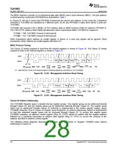
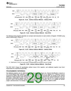
TLK10002
SLLSE75 –MAY 2011
www.ti.com
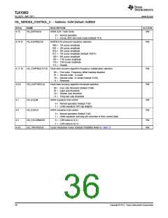
BIT(s)
NAME
DESCRIPTION
ACCESS
RX De-Mux selection control for lane de-serialization on receive channel. Valid only
when RX_MODE_SEL (1.13) is LOW
RW
1.9
RX_DEMUX_SEL
0 = 1 to 2
1 = 1 to 4 (Default 1’b1)
TX Mux selection control for lane serialization on transmit channel. Valid only when
TX_MODE_SEL (1.12) is LOW
RW
RW
1. 8
TX_MUX_SEL
0 = 2 to 1
1 = 4 to 1 (Default 1’b1)
Output clock divide setting. This value is used to divide selected clock (Selected
using CLKOUT_SEL (1.3:2)) before giving it out onto CLKOUTxP/N.
0000 = Divide by 1 (Default 4’b0000)
0001 = RESERVED
0010 = RESERVED
0011 = RESERVED
0100 = Divide by 2
0101 = RESERVED
0110 = RESERVED
0111 = RESERVED
1000 = Divide by 4
1001 = Divide by 8
1010 = Divide by 16
1011 = RESERVED
1100 = Divide by 5
1101 = Divide by 10
1110 = Divide by 20
1111 = Divide by 25
1.7:4
CLKOUT_DIV[3:0]
See Figure 11. Clocking Architecture
Output clock select. Selected Recovered clock sent out on CLKOUTxP/N pins
RW
00 = Selects Channel A HSRX recovered byte clock as output clock (Default
2’b00)
01 = Selects Channel B HSRX recovered byte clock as output clock
10 = Selects Channel A HSRX VCO divide by 2 clock as output clock
11 = Selects Channel B HSRX VCO divide by 2 clock as output clock
See Figure 11. Clocking Architecture
1.3:2
CLKOUT_SEL[1:0]
Channel Reference clock selection. Applicable only when REFCLKx_SEL pin is
LOW.
RW
RW
0 = Selects REFCLK_0_P/N as clock reference to Channel x (Default 1’b0)
1 = Selects REFCLK_1_P/N as clock reference to Channel x
1.1
1.0
REFCLK_ SEL
RESERVED
See Figure 11. Clocking Architecture
For TI use only (Default 1’b0)
32
Copyright © 2011, Texas Instruments Incorporated

 TI [ TEXAS INSTRUMENTS ]