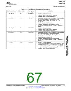
RM46L450
RM46L850
www.ti.com
SPNS184 –SEPTEMBER 2012
4.7 Clock Monitoring
The LPO Clock Detect (LPOCLKDET) module consists of a clock monitor (CLKDET) and an internal low
power oscillator (LPO).
The LPO provides two different clock sources – a low frequency (LFLPO) and a high frequency (HFLPO).
The CLKDET is a supervisor circuit for an externally supplied clock signal (OSCIN). In case the OSCIN
frequency falls out of a frequency window, the CLKDET flags this condition in the global status register
(GLBSTAT bit 0: OSC FAIL) and switches all clock domains sourced by OSCIN to the HFLPO clock (limp
mode clock).
The valid OSCIN frequency range is defined as: fHFLPO / 4 < fOSCIN < fHFLPO * 4.
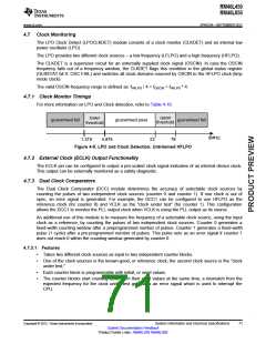
4.7.1 Clock Monitor Timings
For more information on LPO and Clock detection, refer to Table 4-10.
upper
threshold
lower
threshold
guaranteed fail
guaranteed pass
guaranteed fail
f[MHz]
1.375
4.875
22
78
Figure 4-9. LPO and Clock Detection, Untrimmed HFLPO
4.7.2 External Clock (ECLK) Output Functionality
The ECLK pin can be configured to output a pre-scaled clock signal indicative of an internal device clock.
This output can be externally monitored as a safety diagnostic.
4.7.3 Dual Clock Comparators
The Dual Clock Comparator (DCC) module determines the accuracy of selectable clock sources by
counting the pulses of two independent clock sources (counter 0 and counter 1). If one clock is out of
spec, an error signal is generated. For example, the DCC1 can be configured to use HFLPO as the
reference clock (for counter 0) and VCLK as the "clock under test" (for counter 1). This configuration
allows the DCC1 to monitor the PLL output clock when VCLK is using the PLL output as its source.
An additional use of this module is to measure the frequency of a selectable clock source, using the input
clock as a reference, by counting the pulses of two independent clock sources. Counter 0 generates a
fixed-width counting window after a preprogrammed number of pulses. Counter 1 generates a fixed-width
pulse (1 cycle) after a pre-programmed number of pulses. This pulse sets as an error signal if counter 1
does not reach 0 within the counting window generated by counter 0.
4.7.3.1 Features
•
•
Takes two different clock sources as input to two independent counter blocks.
One of the clock sources is the known-good, or reference clock; the second clock source is the "clock
under test."
•
•
Each counter block is programmable with initial, or seed values.
The counter blocks start counting down from their seed values at the same time; a mismatch from the
expected frequency for the clock under test generates an error signal which is used to interrupt the
CPU.
Copyright © 2012, Texas Instruments Incorporated
System Information and Electrical Specifications
Submit Documentation Feedback
Product Folder Links: RM46L450 RM46L850
71

 TI [ TEXAS INSTRUMENTS ]