PCM9211
SBAS495 –JUNE 2010
www.ti.com
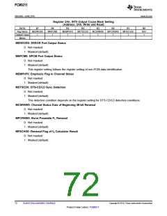
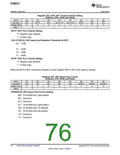
Register 2Eh, INT0, INT1 Output Polarity Setting
(Address: 2Eh, Write and Read)
DATA
Reg Name
Default Value
Memo
B7
RSV
0
B6
INT1P
0
B5
RSV
0
B4
ADLVLTH1
0
B3
ADLVLTH0
0
B2
INT0P
0
B1
RSV
0
B0
RSV
0
INT1P: INT1 Port, Polarity Setting
0: Negative logic (default)
1: Positive logic
ADLVLTH[1:0]: ADC Input Level Detection Threshold for INT1
00: –12dB
:
01: –24dB
10: –36dB
11: –48dB
INT0P: INT0 Port, Polarity Setting
0: Negative logic (default)
1: Positive logic
When the INT0 or INT1 Information Register is read, Register INT0 or INT1 port output is cleared.
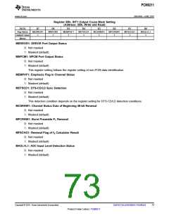
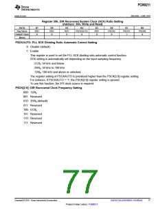
Register 2Fh, DIR Output Data Format
(Address: 2Fh, Write and Read)
DATA
Reg Name
Default Value
Memo
B7
RSV
0
B6
RSV
0
B5
RSV
0
B4
RSV
0
B3
RSV
0
B2
RXFMT2
1
B1
RXFMT1
0
B0
RXFMT0
0
RXFMT[2:0]: DIR Output Data Format Setting
000: 24-bit MSB first, right-justified
001: Reserved
010: Reserved
011: 16-bit MSB first, right-justified
100: 24-bit MSB first, I2S (default)
101: 24-bit MSB first, left-justified
110: Reserved
111: Reserved
76
Submit Documentation Feedback
Copyright © 2010, Texas Instruments Incorporated
Product Folder Link(s): PCM9211

 TI [ TEXAS INSTRUMENTS ]