PCM9211
SBAS495 –JUNE 2010
www.ti.com
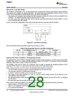
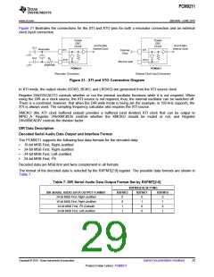
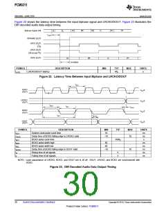
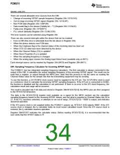
Figure 22 shows the latency time between the input biphase signal and LRCKO/DOUT. Figure 23 illustrates the
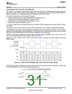
DIR decoded audio data output timing.
Biphase Signal (IN)
W
0R
M
1L
W
1R
B
0L
tLATE
BFRAME (OUT)
LRꢀC (OUT)
(I2S)
LRꢀC (OUT)
(All except I2S)
DATA (OUT)
0L
0R
1L
1R
17 1BꢀC
SYMBOL
tLATE
DESCRIPTION
MIN
TYP
MAX
UNITS
LRCKO/DOUT latency
4/fS
s
Figure 22. Latency Time Between Input Biphase and LRCKO/DOUT
tSCY
SCKO
(OUT)
VDD/2
VDD/2
VDD/2
VDD/2
LRCKO
(OUT)
tBCH
tBCL
tCKLR
BCKO
(OUT)
tBCY
tBCDO
DOUT
(OUT)
SYMBOL
tSCY
DESCRIPTION
MIN
18
TYP
MAX
UNITS
ns
System clock pulse cycle time
Delay time of BCKO falling edge to LRCKO valid
BCKO pulse cycle time
tCKLR
tBCY
tBCH
tBCL
tBCDO
tR
–10
10
ns
1/64fS
s
BCKO pulse width high
60
60
ns
BCKO pulse width low
ns
Delay time of BCKO falling edge to DOUT valid
Rising time of all signals
–10
10
ns
5
5
ns
tF
Falling time of all signals
ns
NOTE: Load capacitance of LRCKO, BCKO, and DOUT pin is 20 pF. DOUT, LRCKO, and BCKO are synchronized with
SCKO.
Figure 23. DIR Decoded Audio Data Output Timing
30
Submit Documentation Feedback
Copyright © 2010, Texas Instruments Incorporated
Product Folder Link(s): PCM9211

 TI [ TEXAS INSTRUMENTS ]