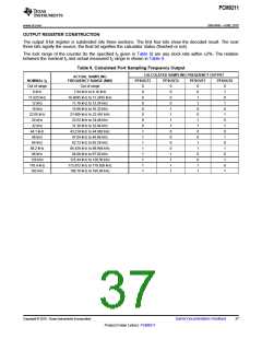
PCM9211
www.ti.com
SBAS495 –JUNE 2010
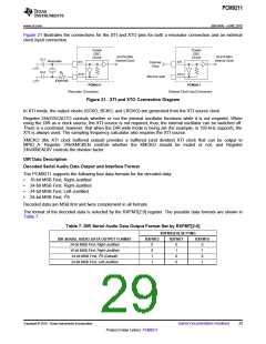
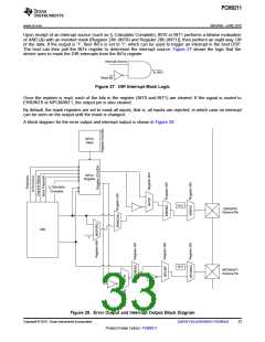
Upon receipt of an interrupt source (such as fS Calculator Complete), INT0 or INT1 performs a bitwise evaluation
of AND (&) with an inverted mask [Register 2Ah (INT0) and Register 2Bh (INT1)], then perform an eight-way OR
of the data. If the output is '1', then INTx is set to '1', which can be used to trigger an interrupt in the host DSP.
The host can then poll the INTx register to determine the interrupt source. Figure 27 shows the logic that the
device uses to mask the DIR interrupts from the INTx register.
Interrupt Source
To INTx
Mask Bit
Figure 27. DIR Interrupt Mask Logic
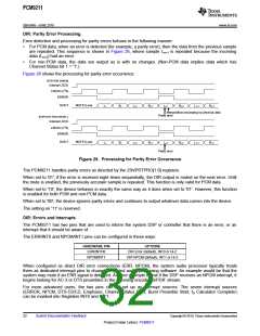
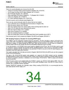
Once the register is read, each of the bits in the register (INT0 and INT1) are cleared. If the signal is routed to
ERR/INT0 or NPCM/INT1, the output pin is also cleared.
By default, the mask registers are set to mask all inputs; that is, all inputs are rejected, in which case no interrupt
can be seen on the output until the mask is changed.
A block diagram for the error output and interrupt output is shown in Figure 28.
INT0/1
Mask
INT0/1
Register
fS Calculator
Complete
Hi-Z
ERR/INT0
External Pin
DIR
‘1’
Hi-Z
NPCM/INT1
External Pin
Figure 28. Error Output and Interrupt Output Block Diagram
Copyright © 2010, Texas Instruments Incorporated
Submit Documentation Feedback
33
Product Folder Link(s): PCM9211

 TI [ TEXAS INSTRUMENTS ]