PCM1794A
www.ti.com.cn
ZHCSEE9B –AUGUST 2004–REVISED DECEMBER 2015
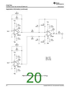
Application Information (continued)
V
DD
MONO
CHSL
DEM
V
2L
1
2
28
27
26
25
24
23
22
21
20
19
18
17
16
15
CC
External
Filter
Device
AGND3L
I
I
L–
L+
3
OUT
WDCK
DATA
BCK
LRCK
DATA
BCK
4
OUT
AGND2
5
V
1
CC
6
Analog
SCK
SCK
V L
COM
7
Output Stage
(See Figure 23)
PCM1794A
DGND
V
COM
R
8
V
DD
I
REF
9
MUTE
FMT0
FMT1
ZERO
RST
AGND1
10
11
12
13
14
I
R–
R+
OUT
I
OUT
AGND3R
V
CC
2R
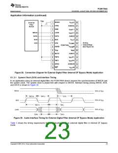
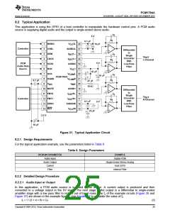
Figure 28. Connection Diagram for External Digital Filter (Internal DF Bypass Mode) Application
8.1.3.1 System Clock (SCK) and Interface Timing
In an application using an external digital filter, the PCM1794A device requires the synchronization of WDCK and
the system clock. The system clock is phase-free with respect to WDCK. Interface timing among WDCK, BCK,
and DATA is shown in Figure 29.
WDCK
50% of V
50% of V
50% of V
DD
DD
DD
t
t
t
(LB)
(BCH)
(BCL)
BCK
t
t
t
(BCY)
(BL)
DATA
t
(DS)
(DH)
Figure 29. Audio Interface Timing for External Digital Filter (Internal DF Bypass Mode) Application
Table 5 shows the timing requirements for an application using an external digital filter in internal DF bypass
mode.
Copyright © 2004–2015, Texas Instruments Incorporated
23

 TI [ TEXAS INSTRUMENTS ]