PCM1794A
ZHCSEE9B –AUGUST 2004–REVISED DECEMBER 2015
www.ti.com.cn
Typical Application (continued)
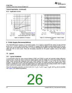
8.2.3 Application Curves
0
−20
10
1
−40
−60
0.1
0.01
−80
−100
−120
−140
−160
0.001
0.0001
0
10 20 30 40 50 60 70 80 90 100
f – Frequency – kHz
−100
−80
−60
−40
−20
0
Input Level – dBFS
VCC = 5 V
TA = 25°C
Measurement circuit is Figure 26
VCC = 5 V
Measurement circuit is Figure 26
fS = 48 kHz, TA = 25°C
fS = 48 kHz, 32768 point 8 average
VDD = 3.3 V
VDD = 3.3 V
–60-db Output Spectrum, BW = 100 kHz
Figure 32. Amplitude vs Frequency
Figure 33. Total Harmonic Distortion + Noise vs Input
Level
9 Power Supply Recommendations
The PCM1794A device requires 5-V (nominal) supplies. A 5-V supply is required for the analog circuitry powered
by the VCC1, VCC2L, and VCC2R pins. A second 5-V supply is for the digital circuitry powered by the VDD pin.
These pins can be powered by the same 5-V rail but separating the supplies can assist with getting the target
SNR and THD in some cases. Place the decoupling capacitors for the power supplies close to the device
terminals.
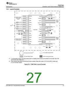
10 Layout
10.1 Layout Guidelines
TI recommends using the same ground between AGND and DGND to avoid any potential voltage difference
between them. Ensure the return currents for digital signals avoid the AGND pin or the input signals to the I/V
stage. Avoid running high frequency clock and control signals near AGND, or any of the IOUT pins where
possible. The pin layout of the PCM1794A partitions into two parts: an analog section and a digital section. If the
system is partitioned in such a way that digital signals are routed away from the analog sections, then no digital
return currents (for example, clocks) should be generated in the analog circuitry.
Place the decoupling capacitors as close to the Vcc1, VCC2L, VCC2R, VCOML, VCOMR, and VDD pins as possible.
See Figure 34 for additional guidelines.
26
Copyright © 2004–2015, Texas Instruments Incorporated

 TI [ TEXAS INSTRUMENTS ]