PCM1794A
www.ti.com.cn
ZHCSEE9B –AUGUST 2004–REVISED DECEMBER 2015
8.2 Typical Application
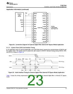
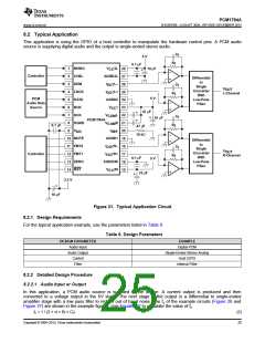
This application is using the GPIO of a host controller to manipulate the hardware control pins. A PCM audio
source is supplying digital audio and the output is single-ended stereo audio.
C
f
5 V
R
f
0.1 µF
MONO
CHSL
DEM
V
2L
1
2
28
27
26
25
24
23
22
21
20
19
18
17
16
15
10 µF
CC
+
–
+
Controller
AGND3L
Differential
to
Single
I L–
OUT
3
C
f
V
OUT
L-Channel
Converter
With
LRCK
DATA
BCK
I
L+
4
OUT
R
f
5 V
PCM
AGND2
Low-Pass
Filter
5
–
+
Audio Data
Source
V
1
CC
6
47 µF
+
+
SCK
V L
COM
7
C
f
+
10 µF
PCM1794A
DGND
V
COM
R
8
R
0.1 µF
f
47 µF
10 kΩ
V
DD
I
REF
9
–
+
MUTE
FMT0
FMT1
ZERO
RST
AGND1
10
11
12
13
14
Differential
to
Single
I
R–
R+
C
f
OUT
V
OUT
R-Channel
Converter
With
Controller
I
OUT
R
f
0.1 µF
5 V
AGND3R
Low-Pass
Filter
–
+
V
CC
2R
10 µF
+
3.3 V
+
10 µF
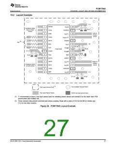
Figure 31. Typical Application Circuit
8.2.1 Design Requirements
For the typical application example, use the parameters listed in Table 6.
Table 6. Design Parameters
DESIGN PARAMETER
Audio Input
Audio Output
Control
EXAMPLE
Digital PCM
Single-Ended Stereo Analog
Host GPIO
Filter
Internal Filter
8.2.2 Detailed Design Procedure
8.2.2.1 Audio Input or Output
In this application, a PCM audio source is supplied to the device. A current output is produced and then
converted to a voltage output in the I/V stage. The next stage in the output is a differential to single-ended
amplifier stage with a low pass filter to reduce out of band noise. The fc of the example circuits (Figure 26 and
Figure 27) are shown in the example figures. Use Equation 2 to calculate the value of fc.
fc = 1 / (2 × π × Rf × Cf)
(2)
Copyright © 2004–2015, Texas Instruments Incorporated
25

 TI [ TEXAS INSTRUMENTS ]