PCM1794A
www.ti.com.cn
ZHCSEE9B –AUGUST 2004–REVISED DECEMBER 2015
8 Application and Implementation
NOTE
Information in the following applications sections is not part of the TI component
specification, and TI does not warrant its accuracy or completeness. TI’s customers are
responsible for determining suitability of components for their purposes. Customers should
validate and test their design implementation to confirm system functionality.
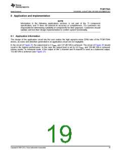
8.1 Application Information
The design of the application circuit lets the user realize the high signal-to-noise (S/N) ratio of the PCM1794A
device, as noise and distortion generated in an application circuit are not negligible.
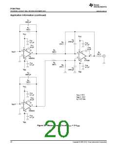
In the circuit of Figure 25, the output level is 2-VRMS, and 127-dB S/N is achieved. The circuit of Figure 26 should
result in the highest performance. In this case the output level is set to 4.5-VRMS, and 129-dB S/N is achieved
(stereo mode). In monaural mode, if the output of the L-channel and R-channel is used as a balanced output,
132-dB S/N is achieved (see Figure 27).
Copyright © 2004–2015, Texas Instruments Incorporated
19

 TI [ TEXAS INSTRUMENTS ]