PCM1794A
www.ti.com.cn
ZHCSEE9B –AUGUST 2004–REVISED DECEMBER 2015
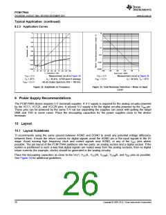
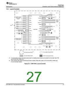
10.2 Layout Example
5 V
+
1
2
28
MONO
CHSL
DEM
V
2L
CC
Hardware select
pins or Host
control
0.1 ꢀF
10 ꢀF
27
26
25
24
23
22
21
20
19
18
17
16
15
AGND3L
Left I/V
Output
circuit
3
I
Lœ
OUT
4
LRCK
DATA
BCK
I
L+
OUTL+
5
AGND2
(2)
See
6
5V
V
1
L
CC
+
+
47 ꢀF
7
SCK
V
COM
10 ꢀF
PCM1794A
3.3 V
+
8
DGND
V
R
COM
10 Kꢁ
9
V
I
REF
0.1 ꢀF
10 ꢀF
DD
10
11
12
13
14
MUTE
FMT0
FMT1
ZERO
RST
AGND1
I
R-
OUT
Right I/V
Output
circuit
Hardware select
or host control
I
R+
OUT
AGND3R
5 V
V
2R
CC
+
0.1 ꢀF
10 ꢀF
(1)
Via to bottom Ground Plane
Pad to top layer ground pour
Top Layer Ground Pour
Top Layer Signal Traces
(1) TI recommends to place a top layer ground pour for shielding around device and connect it to the lower main PCB
ground plane with multiple vias.
(2) These resistors help prevent overshoot and reduce coupling. Begin with a value of 10 Ω for the MCLK resistor and
27 Ω for the other resistors.
Figure 34. PCM1794A Layout Example
版权 © 2004–2015, Texas Instruments Incorporated
27

 TI [ TEXAS INSTRUMENTS ]