PCM1794A
ZHCSEE9B –AUGUST 2004–REVISED DECEMBER 2015
www.ti.com.cn
Application Information (continued)
I
L– (Pin 26)
I
I
–
+
OUT
OUT
OUT+
Figure 25
Circuit
I
L+ (Pin 25)
OUT
OUT
3
2
1
I
I
R– (Pin 18)
I
I
–
+
OUT
OUT
OUT–
Figure 25
Circuit
Balanced Out
R+ (Pin 17)
OUT
OUT
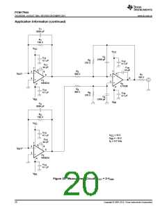
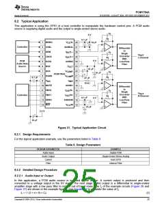
Figure 27. Measurement Circuit for Monaural Mode
8.1.1 I/V Section
The current of the PCM1794A device on each of the output pins (IOUTL+, IOUTL–, IOUTR+, IOUTR–) is 7.8 mA p-p
at 0 dB (full scale). Use Equation 1 to calculate the voltage output level of the I/V converter (Vi).
Vi = 7.8 mA p–p × Rf
where
•
Rf is the feedback resistance of I/V converter
(1)
An NE5534 operational amplifier is recommended for the I/V circuit to obtain the specified performance. Dynamic
performance such as the gain bandwidth, settling time, and slew rate of the operational amplifier affects the
audio dynamic performance of the I/V section.
8.1.2 Differential Section
The PCM1794A voltage outputs are followed by differential amplifier stages, which sum the differential signals for
each channel, creating a single-ended I/V op-amp output. In addition, the differential amplifiers provide a low-
pass filter function.
The operational amplifier recommended for the differential circuit is the Linear Technology LT1028, because the
input noise is low.
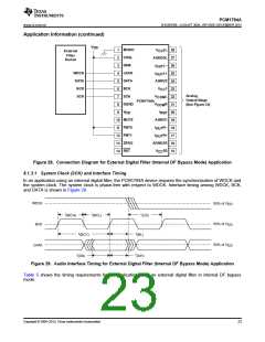
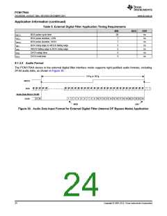
8.1.3 Interfacing With an External Digital Filter
For some applications, using a programmable digital signal processor as an external digital filter to perform the
interpolation function may be necessary. The following pin settings enable the external digital filter application
mode:
•
•
•
•
MONO (pin 1) = LOW
CHSL (pin 2) = HIGH
FMT0 (pin 11) = HIGH
FMT1 (pin 12) = HIGH
The pins that provide the serial interface for the external digital filter are shown in the connection diagram of
Figure 28. The word clock (WDCK) must be operated at 8× or 4× the desired sampling frequency, fS.
22
Copyright © 2004–2015, Texas Instruments Incorporated

 TI [ TEXAS INSTRUMENTS ]