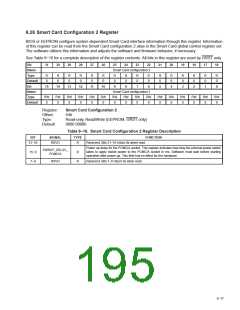
9.26 Smart Card Configuration 2 Register
BIOS or EEPROM configure system dependent Smart Card interface information through this register. Information
of this register can be read from the Smart Card configuration 2 alias in the Smart Card global control register set.
The software utilizes this information and adjusts the software and firmware behavior, if necessary.
See Table 9−16 for a complete description of the register contents. All bits in this register are reset by GRST only.
Bit
31
30
29
28
27
26
25
24
23
22
21
20
19
18
17
16
Name
Type
Default
Bit
Smart Card configuration 2
R
0
R
0
R
0
R
0
R
0
R
0
R
0
9
R
0
8
R
0
7
R
0
6
R
0
5
R
0
4
R
0
3
R
0
2
R
0
1
R
0
0
15
14
13
12
11
10
Name
Type
Default
Smart Card configuration 2
RW
0
RW
0
RW
0
RW
0
RW
0
RW
0
RW
0
RW
0
RW
0
RW
0
RW
0
RW
0
RW
0
RW
0
RW
0
RW
0
Register:
Offset:
Type:
Smart Card Configuration 2
54h
Read-only, Read/Write (EEPROM, GRST only)
0000 0000h
Default:
Table 9−16. Smart Card Configuration 2 Register Description
BIT
SIGNAL
TYPE
FUNCTION
Reserved. Bits 31−16 return 0s when read.
31−16
RSVD
R
Power up delay for the PCMCIA socket. This register indicates how long the external power switch
takes to apply stable power to the PCMCIA socket in ms. Software must wait before starting
operation after power up. This field has no effect for the hardware.
PWRUP_DELAY_
PCMCIA
15−8
7−0
R
R
RSVD
Reserved. Bits 7−0 return 0s when read.
9−17

 TI [ TEXAS INSTRUMENTS ]