9.21 Power Management Data Register
The power management bridge support extension register provides extended power-management features not
applicable to the Smart Card controller; thus, it is read-only and returns 0 when read.
Bit
7
6
5
4
3
2
1
0
Name
Type
Default
Power management data
R
0
R
0
R
0
R
0
R
0
R
0
R
0
R
0
Register:
Offset:
Type:
Power management data
4Bh
Read-only
00h
Default:
9.22 General Control Register
This register controls this function. Information of this register can be read from the socket configuration register in
the Smart Card socket control register set. See Table 9−13 for a complete description of the register contents.
Bit
15
14
13
12
11
10
9
8
7
6
5
4
3
2
1
0
Name
Type
Default
General control
R
0
R
0
R
0
R
0
R
0
R
0
R
0
R
0
R
0
RW
0
RW
0
RW
0
R
0
R
0
R
0
R
0
Register:
Offset:
Type:
General control
4Ch
Read/Write (EEPROM, GRST only)
0000h
Default:
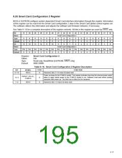
Table 9−13. General Control Register
BIT
FIELD NAME
RSVD
TYPE
R
DESCRIPTION
Reserved. Bits 15−7 return 0s when read.
15−7
6−5 ‡
INT_SEL
RW
Interrupt select. These bits are program the INTPIN register and set which interrupt output is used.
This field is ignored if one of the USE_INTx terminals is asserted.
00 = INTA (pin = 1)
01 = INTB (pin = 2)
10 = INTC (pin = 3)
11 = INTD (pin = 4)
4 ‡
D3_COLD
RSVD
RW
R
Disable function. Setting this bit to 1 hides this function. PCI configuration register of this function
must be accessible at any time. Clock (PCI and 48 MHz) to the rest of the function blocks must be
gated to reduce power consumption.
3−0
Reserved. Bits 3−0 return 0s when read.
‡
One or more bits in this register are cleared only by the assertion of GRST.
9−13

 TI [ TEXAS INSTRUMENTS ]