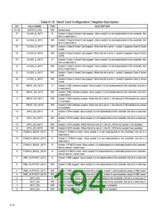
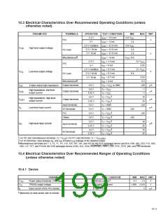
Recommended Operating Conditions (continued)
OPERATION
MIN
0.5 V
NOM
MAX
UNIT
3.3 V
5 V
V
CCP
CCP
PCI
2
V
CCP
V
3.3 V CardBus 0.475 V
3.3 V 16-bit
V
V
V
CC(A/B)
2
CC(A/B)
CC(A/B)
CC(A/B)
High-level input
voltage
†
V
V
V
V
PC Card
V
IH
5 V 16-bit
2.4
PC(0−2)
0.7 V
V
CC
2
CC
CC
‡
Miscellaneous
V
3.3 V
5 V
0
0
0
0
0
0
0
0.3 V
CCP
PCI
0.8
V
3.3 V CardBus
3.3 V 16-bit
5 V 16-bit
0.325 V
CC(A/B)
0.8
†
V
IL
V
V
V
V
Low-level input voltage
PC Card
0.8
PC(0−2)
0.2 V
CC
0.8
‡
‡
‡
Miscellaneous
PCI
0
0
0
V
CCP
PC Card
Miscellaneous
V
CCCB
V
V
Input voltage
V
V
I
V
CC
PCI
0
0
0
V
CC
V
CC
V
CC
4
§
PC Card
Miscellaneous
Output voltage
O
PCI and PC Card
1
0
Input transition time
(t and t )
t
I
ns
t
‡
Miscellaneous
6
r
f
Output current
TPBIAS outputs
−5.6
1.3
mA
O
Cable inputs during data reception
Cable inputs during arbitration
118
168
260
265
Differential input
voltage
V
ID
mV
TPB cable inputs, source power node
TPB cable inputs, nonsource power node
0.4706
0.4706
2.515
Common-mode input
voltage
V
IC
V
¶
2.015
t
Powerup reset time
GRST input
2
ms
PU
S100 operation
1.08
0.5
S200 operation
S400 operation
Receive input jitter
TPA, TPB cable inputs
ns
ns
0.315
S100 operation
S200 operation
S400 operation
0.8
0.55
0.5
Between TPA and TPB
cable inputs
Receive input skew
T
Operating ambient temperature range
Virtual junction temperature
0
0
25
25
70
°C
°C
A
T
J#
115
†
‡
Applies to external inputs and bidirectional buffers without hysteresis
Miscellaneous terminals are 1, 2, 12, 17, 111, 112, 125, 167, 181, and 187 for the PDV packaged device and B10, C09, D01, E03, F12, G03,
H02, L17, P17, and P18 for the GHK packaged device (CNA, SCL, SDA, SUSPEND, GRST, CDx, PHY_TEST_MA, and VSx terminals).
Applies to external output buffers
§
¶
#
For a node that does not source power, see Section 4.2.2.2 in IEEE Std 1394a−2000.
These junction temperatures reflect simulation conditions. The customer is responsible for verifying junction temperature.
10−2

 TI [ TEXAS INSTRUMENTS ]