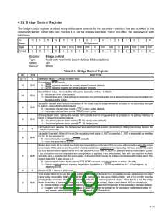
4.32 Bridge Control Register
The bridge control register provides many of the same controls for the secondary interface that are provided by the
command register (offset 04h, see Section 4.3) for the primary interface. Some bits affect the operation of both
interfaces.
Bit
15
14
13
12
11
10
9
8
7
6
5
4
3
2
1
0
Name
Type
Default
Bridge control
R
0
R
0
R
0
R
0
R/W
0
RCU
0
R/W
0
R/W
0
R
0
R/W
0
R/W
0
R
0
R/W
0
R/W
0
R/W
0
R/W
0
Register:
Type:
Bridge control
Read-only, read/write (see individual bit descriptions)
Offset:
Default:
3Eh
0000h
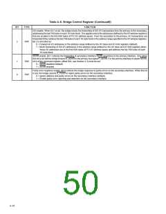
Table 4–6. Bridge Control Register
BIT
TYPE
FUNCTION
15–12
R
Reserved. Bits 15–12 return 0s when read.
Discard timer SERR enable.
11
10
R/W
0 = SERR signaling disabled for primary discard timeouts (default)
1 = SERR signaling enabled for primary discard timeouts
Discard timer status. Once set, this bit must be cleared by writing 1 to this bit.
0 = No discard timer error (default)
RCU
R/W
1 = Discard timer error. Either primary or secondary discard timer expired and a delayed transaction was discarded from
the queue in the bridge.
Secondary discard timer. Selects the number of PCI clocks that the bridge will wait for a master on the secondary interface
to repeat a delayed transaction request.
9
15
0 = Secondary discard timer counts 2 PCI clock cycles (default)
10
1 = Secondary discard timer counts 2 PCI clock cycles
Primary discard timer. Selects the number of PCI clocks that the bridge will wait for a master on the primary interface to
repeat a delayed transaction request.
8
7
6
R/W
R
15
0 = The primary discard timer counts 2 PCI clock cycles (default)
10
1 = The primary discard timer counts 2 PCI clock cycles
Fast back-to-back capable. The bridge never generates fast back-to-back transactions to different secondary devices. Bit
7 returns 0 when read.
Secondary bus reset. When bit 6 is set, the secondary reset signal (S_RST) is asserted. S_RST is deasserted by resetting
this bit. Bit 6 is encoded as:
R/W
0 = Do not force the assertion of S_RST (default).
1 = Force the assertion of S_RST.
Master abort mode. Bit 5 controls how the bridge responds to a master abort that occurs on either interface when the bridge
is the master. If this bit is set and the posted write transaction has completed on the requesting interface, and SERR enable
(bit 8) of the command register (offset 04h, see Section 4.3) is 1, then P_SERR is asserted when a master abort occurs.
If the transaction has not completed, then a target abort is signaled. If the bit is cleared, then all 1s are returned on reads
and write data is accepted and discarded when a transaction that crosses the bridge is terminated with master abort. The
default state of bit 5 after a reset is 0.
5
R/W
0 = Do not report master aborts (return FFFF FFFFh on reads and discard data on writes) (default).
1 = Report master aborts by signaling target abort if possible, or if SERR is enabled via bit 1 of this register, by
asserting SERR.
4
3
R
Reserved. Bit 4 returns 0 when read.
VGA enable. When bit 3 is set, the bridge positively decodes and forwards VGA-compatible memory addresses in the video
frame buffer range 000A 0000h–000B FFFFh, I/O addresses in the range 03B0h–03BBh, and 03C0–03DFh from the
primary to the secondary interface, independent of the I/O and memory address ranges. When this bit is set, the bridge
blocks forwarding of these addresses from the secondary to the primary. Reset clears this bit. Bit 3 is encoded as:
0 = Do not forward VGA-compatible memory and I/O addresses from the primary to the secondary interface (default).
1 = Forward VGA-compatible memory and I/O addresses from the primary to the secondary, independent of the I/O
and memory address ranges and independent of the ISA enable bit.
R/W
4–15

 TI [ TEXAS INSTRUMENTS ]