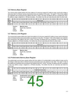
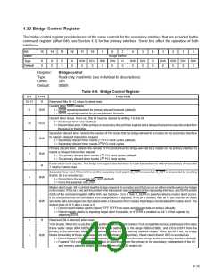
4.20 Memory Base Register
The memory base register defines the base address of a memory-mapped I/O address range used by the bridge to
determine when to forward memory transactions from one interface to the other. The upper 12 bits of this register
are read/write and correspond to the address bits AD31–AD20. The lower 20 address bits are considered 0s; thus,
the address range is aligned to a 1M-byte boundary. The bottom four bits are read-only and return 0s when read.
Bit
15
14
13
12
11
10
9
8
7
6
5
4
3
2
1
0
Name
Type
Default
Memory base
R/W
0
R/W
0
R/W
0
R/W
0
R/W
0
R/W
0
R/W
0
R/W
0
R/W
0
R/W
0
R/W
0
R/W
0
R
0
R
0
R
0
R
0
Register:
Type:
Memory base
Read-only, read/write
Offset:
Default:
20h
0000h
4.21 Memory Limit Register
The memory limit register defines the upper-limit address of a memory-mapped I/O address range used to determine
when to forward memory transactions from one interface to the other. The upper 12 bits of this register are read/write
and correspond to the address bits AD31–AD20. The lower 20 address bits are considered 1s; thus, the address
range is aligned to a 1M-byte boundary. The bottom four bits are read-only and return 0s when read.
Bit
15
14
13
12
11
10
9
8
7
6
5
4
3
2
1
0
Name
Type
Default
Memory limit
R/W
0
R/W
0
R/W
0
R/W
0
R/W
0
R/W
0
R/W
0
R/W
0
R/W
0
R/W
0
R/W
0
R/W
0
R
0
R
0
R
0
R
0
Register:
Type:
Memory limit
Read-only, read/write
Offset:
Default:
22h
0000h
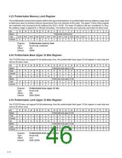
4.22 Prefetchable Memory Base Register
The prefetchable memory base register defines the base address of a prefetchable memory address range used by
the bridge to determine when to forward memory transactions from one interface to the other. The upper 12 bits of
this register are read/write and correspond to the address bits AD31–AD20. The lower 20 address bits are considered
0; thus, the address range is aligned to a 1M-byte boundary. The bottom four bits are read-only and return 0s
when read.
Bit
15
14
13
12
11
10
9
8
7
6
5
4
3
2
1
0
Name
Type
Default
Prefetchable memory base
R/W
0
R/W
0
R/W
0
R/W
0
R/W
0
R/W
0
R/W
0
R/W
0
R/W
0
R/W
0
R/W
0
R/W
0
R
0
R
0
R
0
R
0
Register:
Type:
Prefetchable memory base
Read-only, read/write
Offset:
Default:
24h
0000h
4–11

 TI [ TEXAS INSTRUMENTS ]