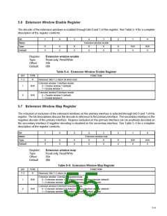
5 Extension Registers
The TI extension registers are those registers that lie outside the standard PCI-to-PCI bridge device configuration
space (i.e., registers 40h–FFh in PCI configuration space in the PCI2250). These registers can be accessed through
configuration reads and writes. The TI extension registers add flexibility and performance benefits to the standard
PCI-to-PCI bridge. The TI extension registers are not reset on the transition from D3 to D0.
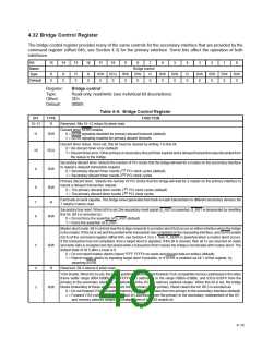
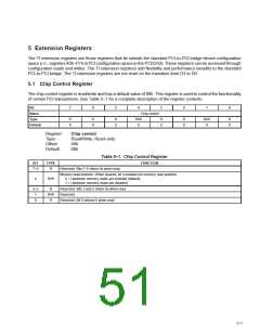
5.1 Chip Control Register
The chip control register is read/write and has a default value of 00h. This register is used to control the functionality
of certain PCI transactions. See Table 5–1 for a complete description of the register contents.
Bit
7
6
5
4
3
2
1
0
Name
Type
Default
Chip control
R
0
R
0
R
0
R/W
0
R
0
R
0
R/W
0
R
0
Register:
Type:
Chip control
Read/Write, Read–only
Offset:
Default:
40h
00h
Table 5–1. Chip Control Register
BIT
TYPE
FUNCTION
7–5
R
Reserved. Bits 7–5 return 0s when read.
Memory read prefetch. When cleared, bit 4 enables the memory read prefetch.
0 = Upstream memory reads are enabled (default)
4
R/W
1 = Upstream memory reads are disabled
3–2
1
R
R/W
R
Reserved. Bits 3 and 2 return 0s when read.
Reserved
0
Reserved. Bit 0 returns 0 when read.
5–1

 TI [ TEXAS INSTRUMENTS ]