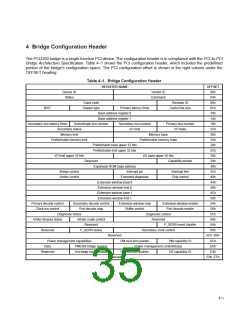
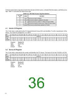
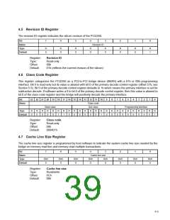
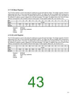
4.5 Revision ID Register
The revision ID register indicates the silicon revision of the PCI2250.
Bit
7
6
5
4
3
2
1
0
Name
Type
Default
Revision ID
R
0
R
0
R
0
R
0
R
0
R
0
R
0
R
1
Register:
Type:
Offset:
Default:
Revision ID
Read-only
08h
01h (reflects the current revision of the silicon)
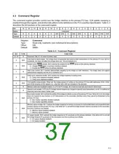
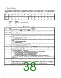
4.6 Class Code Register
This register categorizes the PCI2250 as a PCI-to-PCI bridge device (0604h) with a 01h or 00h programming
interface. Bit 0 is read-only but its value is aliased with bit 0 of the primary decode control register (offset 57h, see
Section 5.9). Bit 0 of the primary decode control register defaults to 1b which means the primary interface is set for
subtractive decode. If software writes a 0 to bit 0 of the primary decode control register, then this value is aliased to
bit 0 of the class code register and the bridge will positively decode the primary interface.
Bit
23 22 21 20 19 18 17 16 15 14 13 12 11 10
9
8
7
6
5
4
3
2
1
0
Name
Class code
Base class
Sub class
Programming interface
Type
R
0
R
0
R
0
R
0
R
0
R
1
R
1
R
0
R
0
R
0
R
0
R
0
R
0
R
1
R
0
R
0
R
0
R
0
R
0
R
0
R
0
R
0
R
0
R
1
Default
Register:
Type:
Offset:
Default:
Class code
Read-only
09h
060401h
4.7 Cache Line Size Register
The cache line size register is programmed by host software to indicate the system cache line size needed by the
bridge on memory read line and memory read multiple transactions.
Bit
7
6
5
4
3
2
1
0
Name
Type
Default
Cache line size
R/W
0
R/W
0
R/W
0
R/W
0
R/W
0
R/W
0
R/W
0
R/W
0
Register:
Type:
Offset:
Default:
Cache line size
Read/write
0Ch
00h
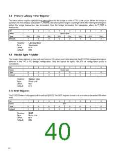
4–5

 TI [ TEXAS INSTRUMENTS ]