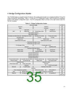
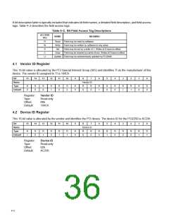
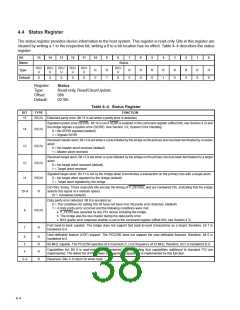
4.4 Status Register
The status register provides device information to the host system. This register is read-only. Bits in this register are
cleared by writing a 1 to the respective bit; writing a 0 to a bit location has no effect. Table 4–4 describes the status
register.
Bit
15
14
13
12
11
10
9
8
7
6
5
4
3
2
1
0
Name
Status
R/C/
U
R/C/
U
R/C/
U
R/C/
U
R/C/
U
R/C/
U
Type
R
0
R
1
R
0
R
0
R
0
R
1
R
0
R
0
R
0
R
0
Default
0
0
0
0
0
0
Register:
Type:
Status
Read-only, Read/Clear/Update
Offset:
Default:
06h
0210h
Table 4–4. Status Register
BIT
TYPE
FUNCTION
15
R/C/U Detected parity error. Bit 15 is set when a parity error is detected.
Signaled system error (SERR). Bit 14 is set if SERR is enabled in the command register (offset 04h, see Section 4.3) and
the bridge signals a system error (SERR). See Section 3.9, System Error Handling.
0 = No SERR signaled (default)
14
13
12
R/C/U
R/C/U
R/C/U
1 = Signals SERR
Received master abort. Bit 13 is set when a cycle initiated by the bridge on the primary bus has been terminated by a master
abort.
0 = No master abort received (default)
1 = Master abort received
Received target abort. Bit 12 is set when a cycle initiated by the bridge on the primary bus has been terminated by a target
abort.
0 = No target abort received (default)
1 = Target abort received
Signaled target abort. Bit 11 is set by the bridge when it terminates a transaction on the primary bus with a target abort.
0 = No target abort signaled by the bridge (default)
11
R/C/U
R
1 = Target abort signaled by the bridge
DEVSEL timing. These read-only bits encode the timing of P_DEVSEL and are hardwired 01b, indicating that the bridge
asserts this signal at a medium speed.
01 = Hardwired (default)
10–9
Data parity error detected. Bit 8 is encoded as:
0 = The conditions for setting this bit have not been met. No parity error detected. (default)
1 = A data parity error occurred and the following conditions were met:
a. P_PERR was asserted by any PCI device including the bridge.
8
7
R/C/U
R
b. The bridge was the bus master during the data parity error.
c. Bit 6 (parity error response enable) is set in the command register (offset 04h, see Section 4.3).
Fast back-to-back capable. The bridge does not support fast back-to-back transactions as a target; therefore, bit 7 is
hardwired to 0.
User-definable feature (UDF) support. The PCI2250 does not support the user-definable features; therefore, bit 6 is
hardwired to 0.
6
5
R
R
R
R
66-MHz capable. The PCI2250 operates at a maximum P_CLK frequency of 33 MHz; therefore, bit 5 is hardwired to 0.
Capabilities list. Bit 4 is read-only and is hardwired to 1, indicating that capabilities additional to standard PCI are
implemented. The linked list of PCI power management capabilities is implemented by this function.
4
3–0
Reserved. Bits 3–0 return 0s when read.
4–4

 TI [ TEXAS INSTRUMENTS ]