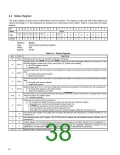
4.3 Command Register
The command register provides control over the bridge interface to the primary PCI bus. VGA palette snooping is
enabled through this register, and all other bits adhere to the definitions in the PCI Local Bus Specification. Table 4–3
describes the bit functions in the command register.
Bit
15
14
13
12
11
10
9
8
7
6
5
4
3
2
1
0
Name
Type
Default
Command
R
0
R
0
R
0
R
0
R
0
R
0
R/W
0
R/W
0
R
0
R/W
0
R/W
0
R
0
R
0
R/W
0
R/W
0
R/W
0
Register:
Type:
Command
Read-only, read/write (see individual bit descriptions)
Offset:
Default:
04h
0000h
Table 4–3. Command Register
BIT
TYPE
FUNCTION
15–10
R
Reserved. Bits 15–10 return 0s when read.
Fast back-to-back enable. The bridge does not generate fast back-to-back transactions on the primary PCI bus. Bit 9 is
read/write, but does not affect the bridge when set. This bit defaults to 0.
9
8
7
6
R/W
System error (SERR) enable. Bit 8 controls the enable for the SERR driver on the primary interface.
0 = Disable SERR driver on primary interface (default)
R/W
R
1 = Enable the SERR driver on primary interface
Wait cycle control. Bit 7 controls address/data stepping by the bridge on both interfaces. The bridge does not support
address/data stepping and this bit is hardwired to 0.
Parity error response enable. Bit 6 controls the bridge response to parity errors.
0 = Parity error response disabled (default)
R/W
1 = Parity error response enabled
VGA palette snoop enable. When set, the bridge passes I/O writes on the primary PCI bus with addresses 3C6h, 3C8h,
and 3C9h inclusive of ISA aliases (i.e., only bits AD9–AD0 are included in the decode).
5
4
3
R/W
R
Memory write and invalidate enable. In a PCI-to-PCI bridge, bit 4 must be read-only and return 0 when read.
Special cycle enable. A PCI-to-PCI bridge cannot respond as a target to special cycle transactions, so bit 3 is defined as
read-only and must return 0 when read.
R
Bus master enable. Bit 2 controls the ability of the bridge to initiate a cycle on the primary PCI bus. When bit 2 is 0, the bridge
does not respond to any memory or I/O transactions on the secondary interface since they cannot be forwarded to the
primary PCI bus.
2
R/W
0 = Bus master capability disabled (default)
1 = Bus master capability enabled
Memory space enable. Bit 1 controls the bridge response to memory accesses for both prefetchable and nonprefetchable
memory spaces on the primary PCI bus. Only when bit 1 is set will the bridge forward memory accesses to the secondary
bus from a primary bus initiator.
1
0
R/W
R/W
0 = Memory space disabled (default)
1 = Memory space enabled
I/O space enable. Bit 0 controls the bridge response to I/O accesses on the primary interface. Only when bit 0 is set will
the bridge forward I/O accesses to the secondary bus from a primary bus initiator.
0 = I/O space disabled (default)
1 = I/O space enabled
4–3

 TI [ TEXAS INSTRUMENTS ]