ꢂ
ꢀꢉ
ꢠ
ꢡ
ꢢ
ꢣ
www.ti.com
SBOS249D − JUNE 2003− REVISED APRIL 2004
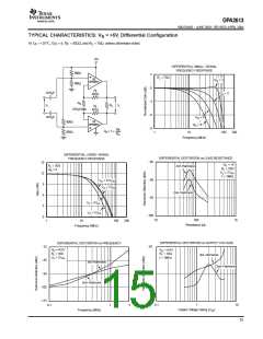
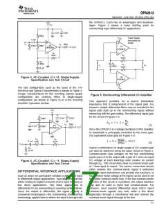
Figure 2 shows the DC-coupled, bipolar supply circuit
configuration used as the basis for the Inverting Gain
−1V/V Typical Characteristics. Key design considerations
of the inverting configuration are developed in the Inverting
Amplifier Operation section.
APPLICATION INFORMATION
WIDEBAND VOLTAGE-FEEDBACK OPERATION
The OPA2613 gives the exceptional AC performance of a
wideband voltage-feedback op amp with a highly linear,
high-power output stage. Requiring only 6mA/ch
quiescent current, the OPA2613 swings to within 1.0V of
either supply rail and delivers in excess of 280mA at room
temperature. This low-output headroom requirement,
along with supply voltage independent biasing, gives
remarkable single (+5V) supply operation. The OPA2613
delivers greater than 20MHz bandwidth driving a 2VPP
output into 100Ω on a single +5V supply. Previous boosted
output stage amplifiers typically suffer from very poor
crossover distortion as the output current goes through
zero. The OPA2613 achieves exceptional power gain with
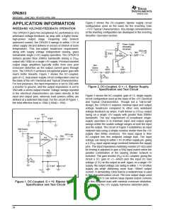
much better linearity. Figure 1 shows the DC-coupled,
gain of +2, dual power-supply circuit configuration used as
the basis of the 6V Electrical and Typical Characteristics.
For test purposes, the input impedance is set to 50Ω with
a resistor to ground; and the output impedance is set to
50Ω with a series output resistor. Voltage swings reported
in the electrical characteristics are taken directly at the
input and output pins, whereas load powers (dBm) are
defined at a matched 50Ω load. For the circuit of Figure 1,
the total effective load is 100Ω || 804Ω = 89Ω.
+5V
Power−Supply
decoupling
not shown.
50 Load
Ω
VO 50Ω
208Ω
1/2
OPA2613
50Ω
Source
−5V
RF
402Ω
RF
402Ω
VI
RM
57.6
Ω
Figure 2. DC-Coupled, G = −1, Bipolar Supply,
Specification and Test Circuit
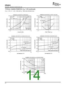
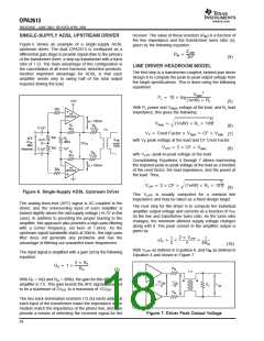
Figure 3 shows the AC-coupled, gain of +2, single-supply
circuit configuration used as the basis of the +5V Electrical
and Typical Characteristics. Though not a “rail-to-rail”
design, the OPA2613 requires minimal input and output
voltage headroom compared to other very wideband
voltage-feedback op amps. It will deliver a 2.6VPP output
swing on a single +5V supply with greater than 20MHz
bandwidth. The key requirement of broadband single-
supply operation is to maintain input and output signal
swings within the usable voltage ranges at both the input
and the output. The circuit of Figure 3 establishes an input
midpoint bias using a simple resistive divider from the +5V
supply (two 806Ω resistors). The input signal is then
AC-coupled into this midpoint voltage bias. The input
voltage can swing to within 1.4V of either supply pin, giving
a 2.2VPP input signal range centered between the supply
pins. The input impedance matching resistor (57.6Ω) used
for testing is adjusted to give a 50Ω input match when the
parallel combination of the biasing divider network is
included. The gain resistor (RG) is AC-coupled, giving the
circuit a DC gain of +1which puts the input DC bias
voltage (2.5V) on the output as well. Again, on a single +5V
supply, the output voltage can swing to within 1.1V of either
supply pin while delivering more than 100mA output
current. A demanding 100Ω load to a midpoint bias is used
in this characterization circuit. The new output stage used
in the OPA2613 can deliver large bipolar output currents
into this midpoint load with minimal crossover distortion,
as shown by the +5V supply, harmonic distortion plots.
+6V
+VS
µ
µ
0.1 F
6.8 F
+
Ω
50 Source
Ω
50 Load
VI
Ω
VO 50
Ω
50
1/2
OPA2613
RF
Ω
402
RG
Ω
402
µ
µ
0.1 F
6.8 F
+
−
VS
−
6V
Figure 1. DC-Coupled, G = +2, Bipolar Supply,
Specification and Test Circuit
16

 TI [ TEXAS INSTRUMENTS ]