OMAP-L137 Low-Power Applications Processor
www.ti.com
SPRS563A–SEPTEMBER 2008–REVISED OCTOBER 2008
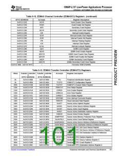
Table 6-8. GPIO Registers (continued)
GPIO
Acronym
Register Description
BYTE ADDRESS
0x01E2 6028
0x01E2 602C
0x01E2 6030
0x01E2 6034
CLR_RIS_TRIG01
SET_FAL_TRIG01
CLR_FAL_TRIG01
INTSTAT01
GPIO Banks 0 and 1 Clear Rising Edge Interrupt Register
GPIO Banks 0 and 1 Set Falling Edge Interrupt Register
GPIO Banks 0 and 1 Clear Falling Edge Interrupt Register
GPIO Banks 0 and 1 Interrupt Status Register
GPIO Banks 2 and 3
0x01E2 6038
0x01E2 603C
0x01E2 6040
0x01E2 6044
0x01E2 6048
0x01E2 604C
0x01E2 6050
0x01E2 6054
0x01E2 6058
0x01E2 605C
DIR23
GPIO Banks 2 and 3 Direction Register
OUT_DATA23
SET_DATA23
CLR_DATA23
IN_DATA23
GPIO Banks 2 and 3 Output Data Register
GPIO Banks 2 and 3 Set Data Register
GPIO Banks 2 and 3 Clear Data Register
GPIO Banks 2 and 3 Input Data Register
SET_RIS_TRIG23
CLR_RIS_TRIG23
SET_FAL_TRIG23
CLR_FAL_TRIG23
INTSTAT23
GPIO Banks 2 and 3 Set Rising Edge Interrupt Register
GPIO Banks 2 and 3 Clear Rising Edge Interrupt Register
GPIO Banks 2 and 3 Set Falling Edge Interrupt Register
GPIO Banks 2 and 3 Clear Falling Edge Interrupt Register
GPIO Banks 2 and 3 Interrupt Status Register
GPIO Banks 4 and 5
0x01E2 6060
0x01E2 6064
0x01E2 6068
0x01E2 606C
0x01E2 6070
0x01E2 6074
0x01E2 6078
0x01E2 607C
0x01E2 6080
0x01E2 6084
DIR45
GPIO Banks 4 and 5 Direction Register
OUT_DATA45
SET_DATA45
CLR_DATA45
IN_DATA45
GPIO Banks 4 and 5 Output Data Register
GPIO Banks 4 and 5 Set Data Register
GPIO Banks 4 and 5 Clear Data Register
GPIO Banks 4 and 5 Input Data Register
SET_RIS_TRIG45
CLR_RIS_TRIG45
SET_FAL_TRIG45
CLR_FAL_TRIG45
INTSTAT45
GPIO Banks 4 and 5 Set Rising Edge Interrupt Register
GPIO Banks 4 and 5 Clear Rising Edge Interrupt Register
GPIO Banks 4 and 5 Set Falling Edge Interrupt Register
GPIO Banks 4 and 5 Clear Falling Edge Interrupt Register
GPIO Banks 4 and 5 Interrupt Status Register
GPIO Banks 6 and 7
0x01E2 6088
0x01E2 608C
0x01E2 6090
0x01E2 6094
0x01E2 6098
0x01E2 609C
0x01E2 60A0
0x01E2 60A4
0x01E2 60A8
0x01E2 60AC
DIR67
GPIO Banks 6 and 7 Direction Register
OUT_DATA67
SET_DATA67
CLR_DATA67
IN_DATA67
GPIO Banks 6 and 7 Output Data Register
GPIO Banks 6 and 7 Set Data Register
GPIO Banks 6 and 7 Clear Data Register
GPIO Banks 6 and 7 Input Data Register
SET_RIS_TRIG67
CLR_RIS_TRIG67
SET_FAL_TRIG67
CLR_FAL_TRIG67
INTSTAT67
GPIO Banks 6 and 7 Set Rising Edge Interrupt Register
GPIO Banks 6 and 7 Clear Rising Edge Interrupt Register
GPIO Banks 6 and 7 Set Falling Edge Interrupt Register
GPIO Banks 6 and 7 Clear Falling Edge Interrupt Register
GPIO Banks 6 and 7 Interrupt Status Register
6.8.2 GPIO Peripheral Input/Output Electrical Data/Timing
Table 6-9. Timing Requirements for GPIO Inputs(1) (see Figure 6-9)
NO.
UNIT
MIN MAX
2C(1)(2)
1
tw(GPIH)
Pulse duration, GPIx high
ns
(1) The pulse width given is sufficient to generate a CPU interrupt or an EDMA event. However, if a user wants to have OMAP-L137
recognize the GPIx changes through software polling of the GPIO register, the GPIx duration must be extended to allow OMAP-L137
enough time to access the GPIO register through the internal bus.
(2) C=SYSCLK4 period in ns. For example, when running parts at 300 MHz, C=13.33 ns
Submit Documentation Feedback
Peripheral Information and Electrical Specifications
97

 TI [ TEXAS INSTRUMENTS ]