OMAP-L137 Low-Power Applications Processor
SPRS563A–SEPTEMBER 2008–REVISED OCTOBER 2008
www.ti.com
6.8 General-Purpose Input/Output (GPIO)
The GPIO peripheral provides general-purpose pins that can be configured as either inputs or outputs.
When configured as an output, a write to an internal register can control the state driven on the output pin.
When configured as an input, the state of the input is detectable by reading the state of an internal
register. In addition, the GPIO peripheral can produce CPU interrupts and EDMA events in different
interrupt/event generation modes. The GPIO peripheral provides generic connections to external devices.
The GPIO pins are grouped into banks of 16 pins per bank (i.e., bank 0 consists of GPIO [0:15]).
The OMAP-L137 GPIO peripheral supports the following:
•
•
Up to 128 Pins on ZKB package configurable as GPIO
External Interrupt and DMA request Capability
–
–
–
–
–
–
Every GPIO pin may be configured to generate an interrupt request on detection of rising and/or
falling edges on the pin.
The interrupt requests within each bank are combined (logical or) to create eight unique bank level
interrupt requests.
The bank level interrupt service routine may poll the INTSTATx register for its bank to determine
which pin(s) have triggered the interrupt.
GPIO Banks 0, 1, 2, 3, 4, 5, 6, and 7 Interrupts assigned to ARM INTC Interrupt Requests 42, 43,
44, 45, 46, 47, 48, and 49 respectively
GPIO Banks 0, 1, 2, 3, 4, 5, 6, and 7 Interrupts assigned to DSP Events 65, 41, 49, 52, 54, 59, 62
and 72 respectively
Additionally, GPIO Banks 0, 1, 2, 3, 4, and 5 Interrupts assigned to EDMA events 6, 7, 22, 23, 28,
and 29 respectively.
•
Set/clear functionality: Firmware writes 1 to corresponding bit position(s) to set or to clear GPIO
signal(s). This allows multiple firmware processes to toggle GPIO output signals without critical section
protection (disable interrupts, program GPIO, re-enable interrupts, to prevent context switching to
anther process during GPIO programming).
•
•
Separate Input/Output registers
Output register in addition to set/clear so that, if preferred by firmware, some GPIO output signals can
be toggled by direct write to the output register(s).
•
Output register, when read, reflects output drive status. This, in addition to the input register reflecting
pin status and open-drain I/O cell, allows wired logic be implemented.
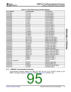
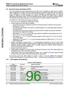
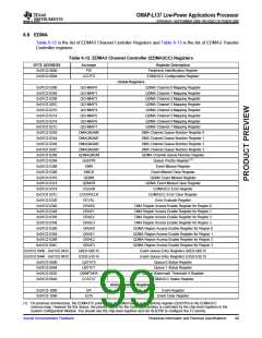
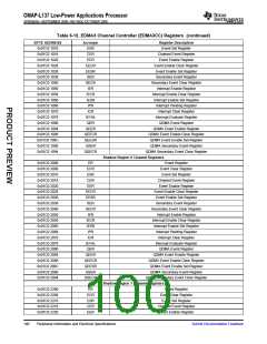
The memory map for the GPIO registers is shown in Table 6-8. See the OMAP-L137 Applications
Processor DSP Peripherals Overview Reference Guide. – Literature Number SPRUGA6 for more details.
6.8.1 GPIO Register Description(s)
Table 6-8. GPIO Registers
GPIO
Acronym
Register Description
BYTE ADDRESS
0x01E2 6000
0x01E2 6004
0x01E2 6008
REV
Peripheral Revision Register
RESERVED
BINTEN
Reserved
GPIO Interrupt Per-Bank Enable Register
GPIO Banks 0 and 1
0x01E2 6010
0x01E2 6014
0x01E2 6018
0x01E2 601C
0x01E2 6020
0x01E2 6024
DIR01
GPIO Banks 0 and 1 Direction Register
GPIO Banks 0 and 1 Output Data Register
GPIO Banks 0 and 1 Set Data Register
GPIO Banks 0 and 1 Clear Data Register
GPIO Banks 0 and 1 Input Data Register
GPIO Banks 0 and 1 Set Rising Edge Interrupt Register
OUT_DATA01
SET_DATA01
CLR_DATA01
IN_DATA01
SET_RIS_TRIG01
96
Peripheral Information and Electrical Specifications
Submit Documentation Feedback

 TI [ TEXAS INSTRUMENTS ]