OMAP-L137 Low-Power Applications Processor
SPRS563A–SEPTEMBER 2008–REVISED OCTOBER 2008
www.ti.com
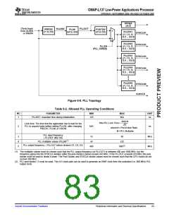
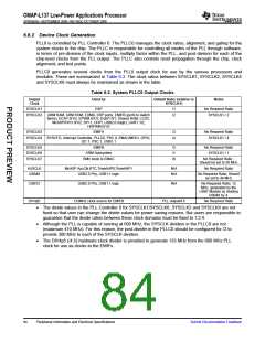
6.6.2 Device Clock Generation
PLL0 is controlled by PLL Controller 0. The PLLC0 manages the clock ratios, alignment, and gating for the
system clocks to the chip. The PLLC is responsible for controlling all modes of the PLL through software,
in terms of pre-division of the clock inputs, multiply factor within the PLL, and post-division for each of the
chip-level clocks from the PLL output. The PLLC also controls reset propagation through the chip, clock
alignment, and test points.
PLLC0 generates several clocks from the PLL0 output clock for use by the various processors and
modules. These are summarized in Table 6-3. The clock ratios between SYSCLK1, SYSCLK2, SYSCLK4
and SYSCLK6 must always be maintained as shown in the table.
Table 6-3. System PLLC0 Output Clocks
Output
Clock
Used by
Default Ratio (relative to
SYSCLK1)
Notes
SYSCLK1
SYSCLK2
DSP
/1
/2
No Required Ratio
SYSCLK1 / 2
ARM RAM, ARM ROM, EDMA, DSP ports, EMIFB (ports to switch
fabric), ECAP 0/1/2, EPWM 0/1/2, EQEP 0/1, Shared RAM, LCDC,
McASP/FIFO 0/1/2, SPI 1, UHPI, USB2.0 (logic), UART 1/2,
HRPWM 0/1/2
SYSCLK3
EMIFA
/3
/4
No Required Ratio
SYSCLK1 / 4
SYSCLK4 SYSCFG, Interrupt Controller, PLLC0, PSC 0, EMAC/MDIO, GPIO,
I2C 1, PSC 1, USB1.1
SYSCLK5
SYSCLK6
SYSCLK7
EMIFB
/3
/1
/6
No Required Ratio
SYSCLK1 / 1
ARM Subsystem
RMII clock to EMAC
No Required Ratio ;
Should be set to 50 MHz
AUXCLK
USB48
McASP AuxClk,RTC,Timer64P0,Timer64P1
USB2.0 Phy, USB1.1 logic
N/A
N/A
No Required Ratio
No Required Ratio; Should
be set to 48 MHz
USB12
USB2.0 Phy, USB1.1 logic
N/A
No Required Ratio; 12
MHz, generated by the
USB1 Module by dividing
USB48 by 4.
DIV4p5
133MHz clock source for EMIFB
PLL output/4.5
No Required Ratio
•
The divide values in the PLL Controller 0 for SYSCLK1/SYSCLK6, SYSCLK2 and SYSCLK4 are not
fixed so that user can change the divide values for power saving reasons. But users are responsible to
guarantee that the divide ratios between these clock domains must be fixed to 1:2:4.
•
•
Although the PLL is capable of running at 600 MHz, the SYSCLK dividers in the PLLC0 are not
(maximum 410 MHz). For this reason, the post-divider in the PLLC0 should be configured for /2 to
provide 300 MHz to each of the SYSCLK dividers.
The DIV4p5 (/4.5) hardware clock divider is provided to generate 133 MHz from the 600 MHz PLL
clock for use as clocks to the EMIFs.
84
Peripheral Information and Electrical Specifications
Submit Documentation Feedback

 TI [ TEXAS INSTRUMENTS ]