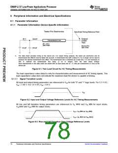
OMAP-L137 Low-Power Applications Processor
SPRS563A–SEPTEMBER 2008–REVISED OCTOBER 2008
www.ti.com
6.6 Clock PLLs
The OMAP-L137 has one PLL controller that provides clock to different parts of the system. PLL0 provides
clocks (though various dividers) to most of the components of the device.
The PLL controller provides the following:
•
•
•
•
Glitch-Free Transitions (on changing clock settings)
Domain Clocks Alignment
Clock Gating
PLL power down
The various clock outputs given by the controller are as follows:
•
•
Domain Clocks: SYSCLK [1:n]
Auxiliary Clock from reference clock source: AUXCLK
Various dividers that can be used are as follows:
•
•
Post-PLL Divider: POSTDIV
SYSCLK Divider: D1, , Dn
Various other controls supported are as follows:
•
•
PLL Multiplier Control: PLLM
Software programmable PLL Bypass: PLLEN
6.6.1 PLL Device-Specific Information
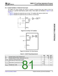
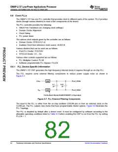
The OMAP-L137 DSP generates the high-frequency internal clocks it requires through an on-chip PLL.
The PLL requires some external filtering components to reduce power supply noise as shown in
Figure 6-7.
CVDD
50R
PLL0_VDDA
0.1
µF
0.01
µF
VSS
50R
PLL0_VSSA
Ferrite Bead: Murata BLMG1P500SPT or Equivalent
Figure 6-7. PLL External Filtering Components
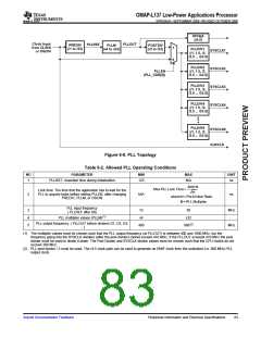
The input to the PLL is either from the on-chip oscillator (OSCIN pin) or from an external clock on the
CLKIN pin. The PLL outputs nine clocks that have programmable divider options. Figure 6-8 illustrates the
PLL Topology.
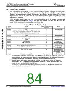
The PLL is disabled by default after a device reset. It must be configured by software according to the
allowable operating conditions listed in Table 6-2 before enabling the DSP to run from the PLL by setting
PLLEN = 1.
82
Peripheral Information and Electrical Specifications
Submit Documentation Feedback

 TI [ TEXAS INSTRUMENTS ]