OMAP-L137 Low-Power Applications Processor
www.ti.com
SPRS563A–SEPTEMBER 2008–REVISED OCTOBER 2008
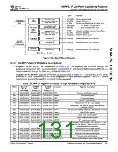
Pins
Function
AHCLKRx Receive Master Clock
Receive Logic
Clock/Frame Generator
State Machine
Peripheral
Configuration
Bus
GIO
Control
ACLKRx
AFSRx
Receive Bit Clock
Receive Left/Right Clock or Frame Sync
The McASPs DO NOT have
dedicated AMUTEINx pins.
AMUTEINx
AMUTEx
Clock Check and
Error Detection
DIT RAM
384 C
384 U
AFSXx
ACLKXx
AHCLKXx
Transmit Left/Right Clock or Frame Sync
Transmit Bit Clock
Transmit Master Clock
Transmit Logic
Clock/Frame Generator
State Machine
Optional
Transmit
Formatter
Serializer 0
Serializer 1
AXRx[0]
AXRx[1]
Transmit/Receive Serial Data Pin
Transmit/Receive Serial Data Pin
McASP
DMA Bus
(Dedicated)
Receive
Formatter
Serializer y
AXRx[y]
Transmit/Receive Serial Data Pin
McASPx (x = 0, 1, 2)
Figure 6-32. McASP Block Diagram
6.15.1 McASP Peripheral Registers Description(s)
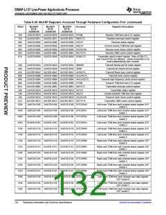
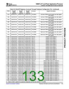
Registers for the McASP are summarized in Table 6-39. The registers are accessed through the
peripheral configuration port. The receive buffer registers (RBUF) and transmit buffer registers (XBUF) can
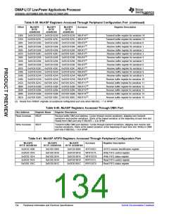
also be accessed through the DMA port, as listed in Table 6-40
Registers for the McASP Audio FIFO (AFIFO) are summarized in Table 6-41. Note that the AFIFO Write
FIFO (WFIFO) and Read FIFO (RFIFO) have independent control and status registers. The AFIFO control
registers are accessed through the peripheral configuration port.
Table 6-39. McASP Registers Accessed Through Peripheral Configuration Port
Offset
McASP0
BYTE
McASP1
BYTE
McASP2
BYTE
Acronym
Register Description
ADDRESS
ADDRESS
ADDRESS
0h
0x01D0 0000
0x01D0 0010
0x01D0 0014
0x01D0 0018
0x01D0 001C
0x01D0 001C
0x01D0 4000
0x01D0 4010
0x01D0 4014
0x01D0 4018
0x01D0 401C
0x01D0 401C
0x01D0 8000 REV
0x01D0 8010 PFUNC
0x01D0 8014 PDIR
0x01D0 8018 PDOUT
0x01D0 801C PDIN
0x01D0 801C PDSET
Revision identification register
Pin function register
10h
14h
18h
1Ch
1Ch
Pin direction register
Pin data output register
Read returns: Pin data input register
Writes affect: Pin data set register (alternate write
address: PDOUT)
20h
44h
48h
4Ch
50h
60h
0x01D0 0020
0x01D0 0044
0x01D0 0048
0x01D0 004C
0x01D0 0050
0x01D0 0060
0x01D0 4020
0x01D0 4044
0x01D0 4048
0x01D0 404C
0x01D0 4050
0x01D0 4060
0x01D0 8020 PDCLR
0x01D0 8044 GBLCTL
0x01D0 8048 AMUTE
0x01D0 804C DLBCTL
0x01D0 8050 DITCTL
0x01D0 8060 RGBLCTL
Pin data clear register (alternate write address: PDOUT)
Global control register
Audio mute control register
Digital loopback control register
DIT mode control register
Receiver global control register: Alias of GBLCTL, only
receive bits are affected - allows receiver to be reset
independently from transmitter
64h
68h
6Ch
70h
74h
0x01D0 0064
0x01D0 0068
0x01D0 006C
0x01D0 0070
0x01D0 0074
0x01D0 4064
0x01D0 4068
0x01D0 406C
0x01D0 4070
0x01D0 4074
0x01D0 8064 RMASK
0x01D0 8068 RFMT
Receive format unit bit mask register
Receive bit stream format register
Receive frame sync control register
Receive clock control register
0x01D0 806C AFSRCTL
0x01D0 8070 ACLKRCTL
0x01D0 8074 AHCLKRCTL
Receive high-frequency clock control register
Submit Documentation Feedback
Peripheral Information and Electrical Specifications
131

 TI [ TEXAS INSTRUMENTS ]