OMAP-L137 Low-Power Applications Processor
www.ti.com
SPRS563A–SEPTEMBER 2008–REVISED OCTOBER 2008
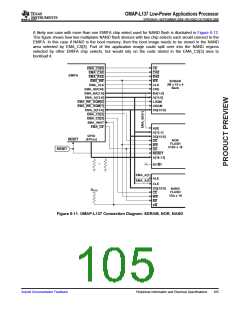
A likely use case with more than one EMIFA chip select used for NAND flash is illustrated in Figure 6-12.
This figure shows how two multiplane NAND flash devices with two chip selects each would connect to the
EMIFA. In this case if NAND is the boot memory, then the boot image needs to be stored in the NAND
area selected by EMA_CS[3]. Part of the application image could spill over into the NAND regions
selected by other EMIFA chip selects; but would rely on the code stored in the EMA_CS[3] area to
bootload it.
EMA_CS[0]
EMA_CAS
CE
CAS
EMIFA
EMA_RAS
RAS
EMA_WE
WE
SDRAM
2M x 16 x 4
Bank
EMA_CLK
CLK
EMA_SDCKE
EMA_BA[1:0]
EMA_A[12:0]
CKE
BA[1:0]
A[11:0]
LDQM
UDQM
DQ[15:0]
EMA_WE_DQM[0]
EMA_WE_DQM[1]
EMA_D[15:0]
EMA_CS[2]
EMA_CS[3]
EMA_WAIT
EMA_OE
A[0]
A[12:1]
DQ[15:0]
CE
GPIO
(6 Pins)
RESET
NOR
FLASH
512K x 16
WE
RESET
OE
RESET
A[18:13]
...
RY/BY
EMA_A[1]
EMA_A[2]
ALE
CLE
DQ[15:0]
CE
NAND
FLASH
1Gb x 16
DVDD
WE
RE
RB
Figure 6-11. OMAP-L137 Connection Diagram: SDRAM, NOR, NAND
Submit Documentation Feedback
Peripheral Information and Electrical Specifications
105

 TI [ TEXAS INSTRUMENTS ]