OMAP-L137 Low-Power Applications Processor
SPRS563A–SEPTEMBER 2008–REVISED OCTOBER 2008
www.ti.com
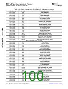
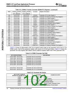
Table 6-13. EDMA3 Transfer Controller (EDMA3TC) Registers (continued)
Offset
Transfer Controller Transfer Controller
Acronym
Register Description
0
1
BYTE ADDRESS
BYTE ADDRESS
310h
314h
340h
344h
348h
34Ch
350h
354h
380h
384h
388h
38Ch
390h
394h
3C0h
3C4h
3C8h
3CCh
3D0h
3D4h
0x01C0 8310
0x01C0 8314
0x01C0 8340
0x01C0 8344
0x01C0 8348
0x01C0 834C
0x01C0 8350
0x01C0 8354
0x01C0 8380
0x01C0 8384
0x01C0 8388
0x01C0 838C
0x01C0 8390
0x01C0 8394
0x01C0 83C0
0x01C0 83C4
0x01C0 83C8
0x01C0 83CC
0x01C0 83D0
0x01C0 83D4
0x01C0 8710
0x01C0 8714
0x01C0 8740
0x01C0 8744
0x01C0 8748
0x01C0 874C
0x01C0 8750
0x01C0 8754
0x01C0 8780
0x01C0 8784
0x01C0 8788
0x01C0 878C
0x01C0 8790
0x01C0 8794
0x01C0 87C0
0x01C0 87C4
0x01C0 87C8
0x01C0 87CC
0x01C0 87D0
0x01C0 87D4
DFBIDX0
DFMPPRXY0
DFOPT1
Destination FIFO B-Index Register 0
Destination FIFO Memory Protection Proxy Register 0
Destination FIFO Options Register 1
DFSRC1
Destination FIFO Source Address Register 1
Destination FIFO Count Register 1
DFCNT1
DFDST1
Destination FIFO Destination Address Register 1
Destination FIFO B-Index Register 1
DFBIDX1
DFMPPRXY1
DFOPT2
Destination FIFO Memory Protection Proxy Register 1
Destination FIFO Options Register 2
DFSRC2
Destination FIFO Source Address Register 2
Destination FIFO Count Register 2
DFCNT2
DFDST2
Destination FIFO Destination Address Register 2
Destination FIFO B-Index Register 2
DFBIDX2
DFMPPRXY2
DFOPT3
Destination FIFO Memory Protection Proxy Register 2
Destination FIFO Options Register 3
DFSRC3
Destination FIFO Source Address Register 3
Destination FIFO Count Register 3
DFCNT3
DFDST3
Destination FIFO Destination Address Register 3
Destination FIFO B-Index Register 3
DFBIDX3
DFMPPRXY3
Destination FIFO Memory Protection Proxy Register 3
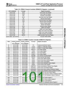
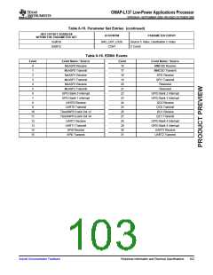
Table 6-14 shows an abbreviation of the set of registers which make up the parameter set for each of 128
EDMA events. Each of the parameter register sets consist of 8 32-bit word entries. Table 6-15 shows the
parameter set entry registers with relative memory address locations within each of the parameter sets.
Table 6-14. EDMA Parameter Set RAM
HEX ADDRESS RANGE
0x01C0 4000 - 0x01C0 401F
0x01C0 4020 - 0x01C0 403F
0x01C0 4040 - 0x01cC0 405F
0x01C0 4060 - 0x01C0 407F
0x01C0 4080 - 0x01C0 409F
0x01C0 40A0 - 0x01C0 40BF
...
DESCRIPTION
Parameters Set 0 (8 32-bit words)
Parameters Set 1 (8 32-bit words)
Parameters Set 2 (8 32-bit words)
Parameters Set 3 (8 32-bit words)
Parameters Set 4 (8 32-bit words)
Parameters Set 5 (8 32-bit words)
...
0x01C0 4FC0 - 0x01C0 4FDF
0x01C0 4FE0 - 0x01C0 4FFF
Parameters Set 126 (8 32-bit words)
Parameters Set 127 (8 32-bit words)
Table 6-15. Parameter Set Entries
HEX OFFSET ADDRESS
WITHIN THE PARAMETER SET
ACRONYM
PARAMETER ENTRY
0x0000
0x0004
0x0008
0x000C
0x0010
0x0014
OPT
SRC
Option
Source Address
A_B_CNT
DST
A Count, B Count
Destination Address
SRC_DST_BIDX
LINK_BCNTRLD
Source B Index, Destination B Index
Link Address, B Count Reload
102
Peripheral Information and Electrical Specifications
Submit Documentation Feedback

 TI [ TEXAS INSTRUMENTS ]