OMAP-L137 Low-Power Applications Processor
SPRS563A–SEPTEMBER 2008–REVISED OCTOBER 2008
www.ti.com
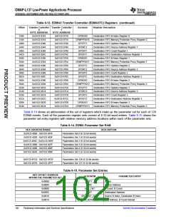
6.10 External Memory Interface A (EMIFA)
EMIFA is one of two external memory interfaces supported on the OMAP-L137 . It is primarily intended to
support asynchronous memory types, such as NAND and NOR flash and Asynchronous SRAM. However
on OMAP-L137 EMIFA also provides a secondary interface to SDRAM.
6.10.1 EMIFA Asynchronous Memory Support
EMIFA supports asynchronous:
•
•
•
SRAM memories
NAND Flash memories
NOR Flash memories
The EMIFA data bus width is up to 16-bits on the ZKB package .The device supports up to fifteen address
lines and an external wait/interrupt input. Up to four asynchronous chip selects are supported by EMIFA
(EMA_CS[5:2]) . All four chip selects are available on the ZKB package.
Each chip select has the following individually programmable attributes:
•
•
•
•
•
•
•
Data Bus Width
Read cycle timings: setup, hold, strobe
Write cycle timings: setup, hold, strobe
Bus turn around time
Extended Wait Option With Programmable Timeout
Select Strobe Option
NAND flash controller supports 1-bit and 4-bit ECC calculation on blocks of 512 bytes.
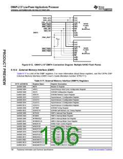
6.10.2 EMIFA Synchronous DRAM Memory Support
The OMAP-L137 ZKB package supports 16-bit SDRAM in addition to the asynchronous memories listed in
Section 6.10.1. It has a single SDRAM chip select (EMA_CS[0]). SDRAM configurations that are
supported are:
•
•
•
•
•
One, Two, and Four Bank SDRAM devices
Devices with Eight, Nine, Ten, and Eleven Column Address
CAS Latency of two or three clock cycles
Sixteen Bit Data Bus Width
3.3V LVCMOS Interface
Additionally, the SDRAM interface of EMIFA supports placing the SDRAM in Self Refresh and Powerdown
Modes. Self Refresh mode allows the SDRAM to be put into a low power state while still retaining memory
contents; since the SDRAM will continue to refresh itself even without clocks from the DSP. Powerdown
mode achieves even lower power, except the DSP must periodically wake the SDRAM up and issue
refreshes if data retention is required.
Finally, note that the EMIFA does not support Mobile SDRAM devices.
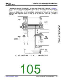
6.10.3 EMIFA Connection Examples
Figure 6-11 illustrates an example of how SDRAM, NOR, and NAND flash devices might be connected to
EMIFA of a OMAP-L137 device simultaneously. The SDRAM chip select must be EMA_CS[0]. Note that
the NOR flash is connected to EMA_CS[2] and the NAND flash is connected to EMA_CS[3] in this
example. Note that any type of asynchronous memory may be connected to EMA_CS[5:2].
The on-chip bootloader makes some assumptions on which chip select the contains the boot image, and
this depends on the boot mode. For NOR boot mode; the on-chip bootloader requires that the image be
stored in NOR flash on EMA_CS[2]. For NAND boot mode, the bootloader requires that the boot image is
stored in NAND flash on EMA_CS[3]. It is always possible to have the image span multiple chip selects,
but this must be supported by second stage boot code stored in the external flash.
104
Peripheral Information and Electrical Specifications
Submit Documentation Feedback

 TI [ TEXAS INSTRUMENTS ]