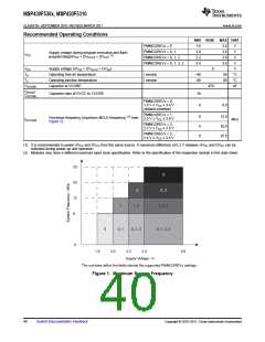
MSP430F530x, MSP430F5310
SLAS677B –SEPTEMBER 2010–REVISED MARCH 2011
www.ti.com
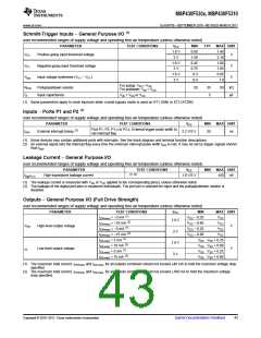
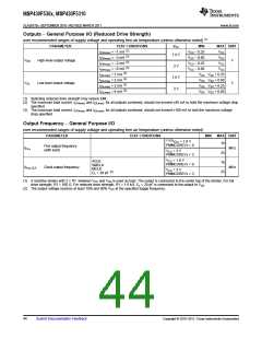
Outputs – General Purpose I/O (Reduced Drive Strength)
over recommended ranges of supply voltage and operating free-air temperature (unless otherwise noted)
(1)
PARAMETER
TEST CONDITIONS
VCC
MIN
CC – 0.25
CC – 0.60
CC – 0.25
CC – 0.60
MAX UNIT
(2)
I(OHmax) = –1 mA
V
V
V
V
VCC
1.8 V
(3)
(2)
(3)
I(OHmax) = –3 mA
I(OHmax) = –2 mA
I(OHmax) = –6 mA
VCC
VOH
High-level output voltage
V
VCC
3 V
1.8 V
3 V
VCC
(2)
I(OLmax) = 1 mA
I(OLmax) = 3 mA
I(OLmax) = 2 mA
I(OLmax) = 6 mA
VSS VSS + 0.25
VSS VSS + 0.60
VSS VSS + 0.25
VSS VSS + 0.60
(3)
VOL
Low-level output voltage
V
(2)
(3)
(1) Selecting reduced drive strength may reduce EMI.
(2) The maximum total current, I(OHmax) and I(OLmax), for all outputs combined, should not exceed ±48 mA to hold the maximum voltage drop
specified.
(3) The maximum total current, I(OHmax) and I(OLmax), for all outputs combined, should not exceed ±100 mA to hold the maximum voltage
drop specified.
Output Frequency – General Purpose I/O
over recommended ranges of supply voltage and operating free-air temperature (unless otherwise noted)
PARAMETER
TEST CONDITIONS
MIN
MAX UNIT
(1)(2)
V
CC
= 1.8 V
16
PMMCOREVx = 0
Port output frequency
(with load)
fPx.y
MHz
25
VCC = 3 V
PMMCOREVx = 3
VCC = 1.8 V
PMMCOREVx = 0
ACLK
SMCLK
MCLK
16
fPort_CLK
Clock output frequency
MHz
25
VCC = 3 V
PMMCOREVx = 3
(2)
CL = 20 pF
(1) A resistive divider with 2 × R1 between VCC and VSS is used as load. The output is connected to the center tap of the divider. For full
drive strength, R1 = 550 Ω. For reduced drive strength, R1 = 1.6 kΩ. CL = 20 pF is connected to the output to VSS
.
(2) The output voltage reaches at least 10% and 90% VCC at the specified toggle frequency.
44
Submit Documentation Feedback
Copyright © 2010–2011, Texas Instruments Incorporated

 TI [ TEXAS INSTRUMENTS ]