MSP430F530x, MSP430F5310
SLAS677B –SEPTEMBER 2010–REVISED MARCH 2011
www.ti.com
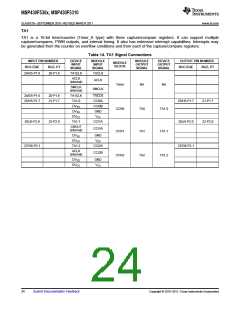
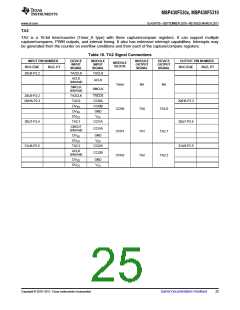
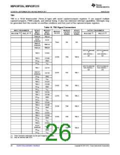
TB0
TB0 is a 16-bit timer/counter (Timer_B type) with seven capture/compare registers. It can support multiple
capture/compares, PWM outputs, and interval timing. It also has extensive interrupt capabilities. Interrupts may
be generated from the counter on overflow conditions and from each of the capture/compare registers.
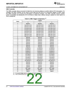
Table 16. TB0 Signal Connections
INPUT PIN NUMBER
DEVICE
INPUT
SIGNAL
MODULE
INPUT
SIGNAL
MODULE
OUTPUT
SIGNAL
DEVICE
OUTPUT
SIGNAL
OUTPUT PIN NUMBER
MODULE
BLOCK
(1)
(1)
(1)
(1)
RGC/ZQE
RGZ, PT
RGC/ZQE
RGZ, PT
TB0CLK
TBCLK
ACLK
(internal)
ACLK
Timer
CCR0
NA
NA
SMCLK
(internal)
SMCLK
TBCLK
TB0CLK
ADC10 (internal) ADC10 (internal)
(2)
(2)
TB0.0
CCI0A
ADC10SHSx =
{2}
ADC10SHSx =
{2}
TB0
TB0.0
TB0.0
DVSS
DVCC
CCI0B
GND
VCC
ADC10 (internal) ADC10 (internal)
TB0.1
CCI1A
ADC10SHSx =
{3}
ADC10SHSx =
{3}
CBOUT
(internal)
CCR1
TB1
TB0.1
CCI1B
DVSS
DVCC
TB0.2
TB0.2
DVSS
DVCC
TB0.3
TB0.3
DVSS
DVCC
TB0.4
TB0.4
DVSS
DVCC
TB0.5
TB0.5
DVSS
DVCC
TB0.6
GND
VCC
CCI2A
CCI2B
GND
CCR2
CCR3
CCR4
CCR5
TB2
TB3
TB4
TB5
TB0.2
TB0.3
TB0.4
TB0.5
VCC
CCI3A
CCI3B
GND
VCC
CCI4A
CCI4B
GND
VCC
CCI5A
CCI5B
GND
VCC
CCI6A
ACLK
(internal)
CCI6B
CCR6
TB6
TB0.6
DVSS
DVCC
GND
VCC
(1) Timer functions selectable via the port mapping controller.
(2) Only on devices with ADC.
26
Submit Documentation Feedback
Copyright © 2010–2011, Texas Instruments Incorporated

 TI [ TEXAS INSTRUMENTS ]